Bronco Webinar 800x100 1

Seeing inside SoC designs, from the beginning

Seeing inside SoC designs, from the beginning
by Don Dingee on 01-31-2013 at 8:10 pm

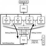
Engineers have this fascination with how things work. They are thrilled to tear stuff apart, and sometimes to even be able to put it back together afterwords. So I can keep my recovering engineer card, I thought I’d take a few moments and look inside a technology Daniel Payne and I have been covering here, exploring where the idea started and how the approach is different.

Continue reading “Seeing inside SoC designs, from the beginning”


Dynamic/Leakage Power Reduction in Memories

Dynamic/Leakage Power Reduction in Memories
by Daniel Nenni on 01-31-2013 at 8:05 pm

Embedded memories have an important impact on power. SoCs that integrate multiple functions on a single silicon die are at the heart of many electronic devices. As process geometries have scaled, design teams have used more and more of the additional silicon real estate available to integrate embedded memories that serve as scratch-pads, FIFOs, and caches to store data for the computational cores. As a result, most current designs have over 50 percent of their area used by embedded memories and these memories account for 50‑70 percent of total SoC power dissipation. Clearly, any attempt to reduce SoC power is incomplete if it does not attempt to reduce the power consumed by the embedded memories in a design.


Given the complexity of today’s SoCs, efficient power management requires a holistic approach where the control logic, data paths, and memories are analyzed together and optimized for both dynamic and static power. However, identifying sequential clock and memory gating opportunities is beyond the scope of RTL synthesis tools. Power conscious designers try to analyze the registers for redundant accesses and look for conditions under which such accesses can be shut off. There is no single known method of achieving this, and designers mostly develop this expertise over time. Even so, the process can get very tedious and error prone without suitable assistance.

In an earlier webinar Calypto presented the concept of deep sequential analysis (DSA) and how it can be used to reduce power at RTL. Sequential analysis involves temporal analysis of the complete design — including gates, flops, and memories — over several clock cycles and the examination of the stability, propagation, and observability of signal values. This is important for power optimization in identifying unused computations, data dependent functions, and don’t-care cycles in the original code.

Sequential analysis is equally applicable to embedded memories. Memories are used to store the results of intermediate computations in the data pipelines; serve as buffers between interacting computations; or serve as caches to store frequently read data. Even though locally the reads and writes to a memory may appear to be necessary, depending on the functional mode or complex control sequence of the design, they may not be needed. Removing such redundant memory accesses can result in significant reduction in the dynamic power consumption of memories.

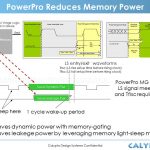
Memory vendors provide several capabilities to reduce leakage power in memories that are not in use, and various flavors of sleep modes are now available in embedded memories, but using these modes requires the creation of controllers to generate the sleep and wake signals. In addition, the leakage power savings gained during sleep mode must be greater than the dynamic power dissipation associated with transitioning the memory in and out of sleep mode. The memory must be in sleep mode for a minimum number of cycles to actually save power. Finally, creating the sleep mode control signals and ensuring that sleep modes are triggered only during periods when the memory is quiet for an extended period require analysis of the design functionality over multiple cycles. DSA is very effective in analyzing and identifying optimum sleep modes for embedded memories.

In their next webinar Calypto will show how its patented deep sequential analysis (DSA) technology can be applied to reduce memory power. Deep sequential analysis examines the read and write operation of memories over several cycles and automatically optimizes the memories for both dynamic and leakage power. It also implements optimized sleep modes for the memory.


TSMC ♥ Oasys

TSMC ♥ Oasys
by Paul McLellan on 01-31-2013 at 8:05 pm

Oasys has joined the TSMC Soft-IP Alliance Program. This means that TSMC IP partners have access to a new RTL exploration tool to improve QoR and reduce the iterations needed for design closure. In modern process nodes, RTL engineers implementing complex IP cores for graphics, networking, and mobile computing are struggling with new QoR and time to market issues.

RealTime Explorer enables RTL engineers to have a physically aware, implementation accurate synthesis tool for top-level PPA and routing analysis without requiring them to be physical design experts. Without an accurate tool like RealTime Explorer, RTL designers either ignore physical design issues and their impact on timing and physical issues such as congestion. Or else they have to go through a complete iteration of physical design which can take days, even assuming that tools and physical design engineers are available to perform the work.

One feature that makes a big productivity difference is the logical-to-physical cross-probing capability that makes it easy to get at the root cause of timing and routing issues before even handing the design off for physical design. It is simple to go straight from the violation in the physical domain and connect straight back to the line(s) of RTL that originate the problem.


Advanced Technology-Design-Manufacturing Co-optimization

Advanced Technology-Design-Manufacturing Co-optimization
by Daniel Nenni on 01-31-2013 at 7:00 pm

I spent some quality time with Subi Kengeri, Vice President, Technology Architecture, Office of the CTO, GLOBALFOUNDRIES in Las Vegas during CES. Great guy, he worked at Silicon Access, Virage and TSMC before GF. One thing you should know about embedded memory guys, SRAM is the first thing that goes through a new process so they know their process technologies.

At Silicon Access Networks, Subi Directed a WW Engineering team to a first pass silicon sucess on industry’s first 10G classification processor SoC. At Virage, with responsibilities of WW design centers and advanced memory R&D, Subi took the Company to a leadership position on 90nm, 65nm and 40nm nodes. At TSMC, Subi was the Sr. Director in Design and Technology Platform and the Head of their North America Design Center. With a large engineering team in the US and Taiwan, Subi was responsible for technology enablement of advanced nodes and interfaced with strategic customers and partners.
Subi also has 30+ patents.

At GF, Subi is responsible for determining the technology feasibility, competitiveness and manufacturability of all elements of technology platform and to establish the advanced technology (14nm) roadmap. Subi is also one of the presenters at the Common Platform Technology Forum next week at the Santa Clara Convention Center:

[TABLE]
|-
| valign=”top” |
| valign=”top” | 2:50pm – 3:50pm
| valign=”top” |
| valign=”top” | Advanced Technology-Design-Manufacturing Co-optimization — A Triathlon

  • Subramani Kengeri, Vice President, Technology Architecture, Office of the CTO, GLOBALFOUNDRIES
  • Joe Sawicki, Vice President & General Manager, Design-to-Silicon Division, Mentor Graphics

This session explores the challenges of bringing advanced technology into high volume manufacturing. Similar to a Triathlon, there are three legs: Technology Architecture Development, Design Enablement and Manufacturing Ramp. Careful co-optimization of the interactions among all three disciplines is required at each stage of the process node maturity cycle. This technical session delves into critical requirements, challenges and solutions to enable SoC level product value and accelerated Time-to-Volume at current and future nodes, and touches on new approaches such as multi-patterning, FinFETs and IC reliability checking.
|-

Subi will start off with a quick overview of broad requirements that drive Foundry Technology which calls for deep collaboration with market drivers. Some areas of system design and technology collaboration will be discussed. Extending Mike Noonen’s point on changing landscape in the Mobile industry, Subi will touch upon the impact to foundry business and technology requirements before discussing details of two major challenges ahead: Device Architecture and Lithography.

Next he will go into details of critical technology considerations for mobile applications with focus on power density and EM issues. He will explain the technology architecture options for reducing active and standby power in SoCs. This will lead into a discussion on why FinFET architecture requires very careful focus of parasitic modeling, EM-aware standard cell design and metrology to ensure optimization of critical SoC metrics and volume ramp. With first generation FinFET architected for time-to-volume, he will discuss how GF is leveraging their HKMG Production ramp. Further, all the SoC level optimizations done on 20nm planar, which gave it ~15% competitive area advantage, are being carried over to 14XM. He will show a comparison of critical metrics between 28nm, 20nm and 14XM that will highlight the key values of GLOBALFOUNDRIES offerings.

In the third section, Subi will go over 14XM development status and all the technology risk mitigation approaches we are using to bring up first generation FinFET into high volume quickly. Also, Subi will summarize ecosystem readiness for advanced technologies and then provide a view of the 10nm and 7nm technology roadmap. The talk will end with the importance of packaging technologies and show the GF roadmap for the next few generations.

I hope to see you there! Join me for lunch!


Building Energy-Efficient ICs from the Ground Up

Building Energy-Efficient ICs from the Ground Up
by Daniel Payne on 01-31-2013 at 6:02 pm

My oldest son just upgraded Smart Phones from a 3″ display to a 4.5″ display and was shocked to discover that his battery barely lasted 8 hours, so I welcomed him to the reality of limited battery life in modern SoC-based mobile devices. There is some hope in increasing battery life for our consumer-oriented devices and the engineers at Cadence make a case for this in a White Paper: Building Energy-Efficient ICs from the Ground Up.

Continue reading “Building Energy-Efficient ICs from the Ground Up”


Going to DAC 2013 in Austin? The Country’s Best Barbecue is a 20 Minute Walk

Going to DAC 2013 in Austin? The Country’s Best Barbecue is a 20 Minute Walk
by Paul McLellan on 01-30-2013 at 8:05 pm

Going to DAC? I just booked my plane ticket last weekend since flights from the Bay Area to wherever DAC is are so often overbooked. It’s in Austin this year in case you’ve been living under a rock. There are lots of reasons to go, from the academic conference to the world’s biggest EDA exhibition. And here is one more: barbecue.

The Austin area is famous for great barbecue. But you used to need a car (and a lot of time) to really experience the best and make your road trips to Lexington, Lockhart, Luling, Llano, and more. But now there is Franklin Barbecue in downtown Austin. Bon Appétit magazine reckons it is the best in America.

It is at 900 East 11th Street which is a 20 minute walk from the convention center (work up an appetite). They open at 11am but you can expect lines. They stop serving when they run out of food which is around 1pm.

My son was recently sent to Austin to help open an office there. He said it is far and away the best barbecue he’s ever had but you really do need to be prepared to wait an hour to get it. The line starts at 9am and can be hundreds of people long. Make sure to say it is your first time there and if you are lucky they’ll give you samples of all the other stuff you didn’t order. To make sure you come back next time.

They are only open for lunch but they are closed on Mondays. So go and see the exhibits and all the other good stuff at DAC on Monday. Their website is here.

Anthony Bourdain was there:


Catch Jasper at SemiIsrael Verification Day and at DVCon 2013

Catch Jasper at SemiIsrael Verification Day and at DVCon 2013
by Paul McLellan on 01-30-2013 at 4:08 pm

Jasper is presenting at both ends of the world at both ends of February.

First in Israel, it is SemiIsrael Verification Day 2013 on February 5th (next Tuesday) at Green House in Tel Aviv.

  • Zihad Hanna, VP of Research and Chief Architect and General Manager of Jasper Israel will be talking about Security Formal Verification of Hardware Design. I assume this will cover similar ground to the presentation from Haifa Verification conference that I already blogged about. That is at noon.
  • Then at 12.50pm, Mody Miller, Verification Manager at Broadcom will talk about Verifying Connectivity Across SoCs Using Jasper Formal Technology. He is in the unwelcome position of having the last presentation before lunch.

The website for the SemiIsrael Verification Day, including links to register, is here.

Then from February 25th to 28th it is DVCon in San Jose at the DoubleTree Hotel. Hotel rates for DVCon are discounted through tomorrow, Friday.

  • On Tuesday February 26th from 9-10.30am Rajeev Ranjan will present on Verification Coverage Metrics in Formal Verification and Speeding Verification Closure with UCIS Coverage Interoperability Standard. Details on the UCIS session are here. (UCIS is the Unified Coverage Interoperability Standard).
  • On Thursday afternoon of February 28th from 1.30pm until 5pm Lawrence Loh will give a tutorial on A Formal Approach to Low-power Verification. Full details, including an abstract of the tutorial, are here.

Jasper will also be exhibiting at booth 601. The exhibits will be open from 3.30pm to 6.30pm on Tuesday 26th and Wednesday 27th. Drop by to see demos of JasperGold Apps.

The DVCon website, including a links to register and for those discounted hotel rates if you are not local, is here.

Video introduction to DVCon (3 mins):


Virtuoso is 20nm-ready

Virtuoso is 20nm-ready
by Paul McLellan on 01-30-2013 at 1:47 pm

I already talked about how Cadence is splitting Virtuoso into two. Anyway, it is now officially announced. The 6.1 version will continue to be developed as a sort of Virtuoso classic for people doing designs off the bleeding edge that don’t require the new features. And a new Virtuoso 12.1 intended for people doing 20nm and below known as Virtuoso Advanced Node. I’m going to call it VAN for short, although I don’t think that is any sort of official name for it.

I sat down with Steve Lewis (it’s always odd doing press events with people that used to work for me) to get more details.

Major releases of Virtuoso (the first digit changing from 5 to 6 for example) have involved major incompatibilities in the database and SKILL libraries. This has contributed to a very slow transition in the customer base. But great care has been taken here so that 6.1 and 12.1 use the same OA database compatible and SKILL compatible. After all, if you are doing 20nm design, you haveto transition to 12.1.

Obviously one thing is that VAN does is has full support for double patterning. I’ve blogged so much about double patterning recently that I’m going to assume everyone already knows about it and about the sort of features that VAN has to have to support it properly. Instead, I’m going to look at two other big issues in 20nm and below: layout dependent effects (LDE) and local interconnect.

In 20nm, the design rules are much less pass-fail than they used to be. The most dramatic LDE is well-proximity effect. There is a minimum distance that a transistor must be from a well edge. But if the transistor is not going to be affected electrically by being near the well edge then it needs to be much further away. Or else you have to analyze the effect and make sure everything is still OK since these are not second or third order effects, they have significant impact.

One thing that VAN does is to blur the old distinction between Composer (schematic) and layout. The old model was that the circuit designer would create the schematic and then throw it over the wall (or often the ocean) to the layout designer to implement it. That doesn’t work in 20nm because there are too many LDEs. In VAN it is now possible to put some layout information into the schematic and then do a sort of hybrid analysis using layout information where it is provided and schematic data where there isn’t. They call this variability-aware-design.

In particular, the layout is analyzed including all the LDE such as well-proximity. Then when the layout designer finally creates the full design, there is lots of layout data already included at varying levels of detail. It reminds me of the same issues 10 years ago in synthesis requiring physical information and it has some of the same issues. Just as the RTL designers didn’t know much about P&R and vice-versa, the circuit designers don’t know much about layout and the layout people don’t know much about circuit design. But analog design is becoming much more like RF design, where the actual layout has always been the design and there has never been the notion that schematic and layout could be kept completely separate.


Another new thing at 20nm is local interconnect. This is an interconnect layer between the transistor level and metal1. In the fab world, the part of the process that creates the transistors is known as front end of line or FEOL (nothing to do with what EDA calls front-end design). The interconnect and via part of the process is called back end of line or BEOL. So now we have the interesting oxymoron of middle end of line or MEOL. Local interconnect has very strict design rules and, since it is contactless and connects to whatever it passes over it also has very limited use. But within standard cells and other small designs, it can make a big difference to both area and performance.


This means that at 20nm and below there are new challenges for the router to make use of local interconnect when possible.

Obviously, one other feature in VAN is support for FinFETs. This mostly affects extraction rather than requiring a sea-change in how layout is done.

There are lots of other little details, like fractured vias (created from multiple layers of local interconnect for example) and support for some of the other complicated 20nm and below design rules.

Download Cadence’s white paper on 20nm custom and analog design here.


Mentor Snags Two Awards at DesignCon

Mentor Snags Two Awards at DesignCon
by Beth Martin on 01-29-2013 at 8:44 pm

Oh, awards season! The glitz! The glamour! The most important and innovative new design products!

That last part is a key feature of the annual DesignVision awards and the Best in Test awards presented at DesignCon 2013. Mentor Graphics’ test products scored two wins: a DesignVision award for their new Tessent IJTAG product, and a Best in Test award for cell-aware (aka cell-internal) testing. While electronics industry awards may not offer the highest fashion, they do tell you what’s hot, and that’s often worth knowing.

Tessent IJTAG was recognized for enabling the new standard for the access and control of embedded IP, IEEE P1687, or IJTAG to its friends.

Some short overviews of the IJTAG standard are hereand here. Basically, IJTAG can create plug-n-play networks for IP, replacing ad-hoc and proprietary IP interfaces with a standardized interface. Mentor’s IJTAG software provides automation for the standard, so you can easily integrate any IEEE P1687-compliant IP into your design. This is a big deal, and translates into direct time and money savings from reduced test time and smaller tester memory requirements.

The Tessent IJTAG tool reads P1687 files and validates that the components are properly connected to the top-level access point. It then retargets IP-level procedural descriptions to the top-level and translates the results into Verilog test bench language and standard test vector formats like WGL, STIL or SVF. For a more detailed description of IJTAG and Mentor’s Tessent IJTAG, check out this Mentor whitepaper.

If that weren’t exciting enough, Mentor also won a Best in Test award for Tessent TestKompress with Cell-Aware ATPG. Cell-aware is a method by which the cell internals are characterized and modeled so ATPG can find defects that occur within the standard cells. Traditional fault models are abstractions of expected defect behavior and mostly target faults at the cell boundary. But with recent fabrication technologies, more than half of defects can occur within cells, which requires new cell-aware fault models that are based on analysis of the impact of defects within cell layouts.

The Mentor software automates the cell library characterization and offers a modeling syntax, UDFM (user-defined fault model). The cell internal fault models are automatically incorporated into TestKompress pattern generation using UDFM. In fact, you can use the UDFM capability to define any proprietary fault model you want, thus boosting the test quality for your specific process or application.

The cell-aware methodology Mentor devised ensures extremely high quality test patterns because it uses the physical characterization of cells to generate test pattern deterministically for potential defect locations. Mentor published some high-volume production test results with AMD proving that cell-aware testing significantly improves defect coverage and as such reduces defect rates of delivered IC significantly. You can download a paper they did with AMD at the last International Test Conference here (registration needed). The Mentor whitepaper on UDFM and the cell-aware methodology is here.


Improving Methodology the NVIDIA Way

Improving Methodology the NVIDIA Way
by Paul McLellan on 01-29-2013 at 2:57 pm

I was at DesignCon in Santa Clara today and listened to Jonah Alben of NVIDIA’s keynote on what their approach is to improving design methodology. He started by pointing out that most companies underinvest in EDA (and he includes NVIDIA in this). Partially it is complaceny: that last chip taped out so we know we can do it again. Partially it is getting used to the quirks of the methodology: we don’t want to change. And partially it is a tradeoff since people working on methodology are not working directly on the product.

His rules for methodology improvement are:

  • Promote “defend your productivity” mentality (egineers should complain more).
  • Define a long-term direction (and avoid the “this must be fixed right now” mentality).
  • Pick the most important task for near-term investment
  • Every project should do something to improve the methodology (even though in the short-term that might not help that project)
  • Explicitly allocate resources to methodology (or it won’t happen)
  • Involve the product engineers (don’t let the methodology get too remote from actual development).
  • Keep the lights on (don’t try and cut over from the existing methodology to new in one go, you need to keep the old methodology up and running too).

He then talked a bit about what NVIDIA are doing for GPU accelerated EDA, in particular for logic simulation. The problem is that in 4 years you have a design that is 4 times bigger (two nodes of Moore’s law) and 4 years improvement in CPU improvement, which leads to 3.4X longer simulations.

Working with Synopsys on VCS using an NVIDIA K10 running 2 jobs per K10. They get 5X speedup on the GPU which, with all the testbench results in an overall speedup of 2.8X. This isn’t just experimental, it is in actual use at NVIDIA.

Working with Rocketick on gate-level simulation used as part of ATPG, with 2 jobs per K10, they get 17.1X speedup. On one next generation GPU design they sped up test-generation from 20.7 days to 16 hours. Again this is being used in NVIDIA for production use.