Bronco Webinar 800x100 1

Get the Latest Info on DFM at the SPIE Litho Conference

Get the Latest Info on DFM at the SPIE Litho Conference
by glforte on 01-29-2013 at 2:12 pm

While the SPIE Advanced Lithography conference is best known for IC manufacturing, computational lithography, mask preparation and other back-end topics, there is also a significant amount of interest in Design for Manufacturing (DFM) at the conference because some litho issues are best (or only) addressed by modifying the physical design or layout. At the upcoming SPIE Conference (Feb 24-28, San Jose Convention Center), Mentor will present three papers on DFM:

  • Pioneering an on-the-fly simulation technique for the detection of layout-dependent effects during IC design phase, Amr M. S. T. Abdelwahed, Mentor Graphics Egypt (Egypt); Rami Fathy, Mentor Graphics Corp. (Canada); Ahmed Ramadan, Mentor Graphics Egypt (Egypt), 27 February 2013 • 2:40 – 3:00 PM
  • A novel algorithm for automatic arrays detection in a layout, Marwah Shafee, Mentor Graphics Egypt (Egypt); Jea-Woo Park, Ara Aslyan, Juan Andres Torres, Mentor Graphics Corp. (United States); Kareem Madkour, Mentor Graphics Egypt (Egypt)Wael ElManhawy, Mentor Graphics Corp. (United States), 28 February 2013 • 11:50 PM – 12:10 AM
  • Model-based hints for litho-hotspot fixing beyond 20nm node, Jae-Hyun Kang, SAMSUNG Electronics Co., Ltd. (Korea, Republic of); Sarah Mohamed, Mentor Graphics Egypt (Egypt); Wael ElManhawy, Mentor Graphics Corp. (United States); Byung-Moo Kim, Naya Ha, SAMSUNG Electronics Co., Ltd. (Korea, Republic of); Hung Bok Choi, Kee Sup Kim, SAMSUNG Electronics Co., Ltd. (Korea, Republic of); Jean-Marie Brunet, Joe Kwan, Mentor Graphics Corp. (United States); Kareem Madkour, Mentor Graphics Egypt (Egypt); Evan Lee, Mentor Graphics Korea (Korea, Republic of), 28 February 2013 • 3:30 – 3:50 PM

You might want to catch these live and talk to the authors. Alternately, you can access them through this SPIE link http://spie.org/x14168.xml or the IEEE technical library service. For a list of all 13 Mentor papers at SPIE, click here.


Design team in China also lead Network-on-Chip adoption…

Design team in China also lead Network-on-Chip adoption…
by Eric Esteve on 01-29-2013 at 10:43 am

I have mentioned NoC adoption explosion during the last two years, illustrated by the huge growth in revenue of a company like Arteris: if we consider only revenue coming from upfront license sales (not including royalties), Arteris growth has been geometric between 2011 and 2010, passing from 18 to 39 customers, which is more than 2X. This penetration has been consolidated in 2012, as Arteris enjoys more than 50 customers. To summarize:

  • Arteris had 50 CUSTOMERS total as of 2012.
  • And well over 100 design licenses total (cumulative)

To better understand the performance, just remember that Network-on-Chip was a concept in the early 2000’s and the first commercial product was sold in 2006. This adoption rate can be compared with the emergence of Chinese chip design companies: very few were active in the early 2000’s, and then we have seen an explosion of start-up emerging in the mid-2000 and now several of this start-up has turned into well-established chip makers like NuFront, RockChip or Actions Semiconductor.


These three fabless companies have many similarities: they have launched complexes ARM based SoC in 40nm, targeting high volume market segment like Mobile (Handset or Media Tablet) or Set-Top-Box and… they have integrated a NoC from Arteris! The NoC penetration in China is a strong signal: it means that Chinese fabless are playing in the same space than the Nvidia, Qualcomm or Samsung. It also means that the Network-on-Chip, just a concept ten years ago, is penetrating every segment, every region of the world. One reason can be found in Rockchip quote from Li Shiqin: “We evaluated all the leading interconnect technologies and proved that Arteris’ NoC technology is the good choice for our multicore ARM-based SoCs,” said Li Shiqin, IC Design Manager at Rockchip. “Arteris FlexNoC is the suitable way for us to meet our design frequency, power, memory efficiency and QoS requirements.”

Last November, I had the opportunity, during ARM TechCon in Santa Clara, to discuss face to face with Kurt Shuler,

VP of Marketing at Arteris, and Kurt give me his feedback about the numerous customer visits he had in China. He has been really impressed by the energy and enthusiasm of the designers he has met there. Even if the team leader is usually older, quite often coming back home after starting his career in the US, most of the designers are young people, eager to learn new skills and practices. When Kurt describe the atmosphere during these working sessions in China, this sounds me like during the 80’s in Europe, or even more accurate, in the Silicon valley. Just use a X6 multiplication factor, taking into account the 1.343.239.923 population (estimated in 2011), and you realize how much design power these Chinese fabless companies will have soon.

I had a look at a couple of SoC from Nufront and RockChip supporting smartphone, media tablet or STB, and I have noticed that there is still room for new business for IP vendors. In fact, I did not see any MIPI IP interface being specified (and my feeling is that there is no MIPI interface supported), and if some of these SoC support several USB (up to three), none is supporting SuperSpeed USB. I can easily understand why there is no MIPI in the already released SoC: it can be seen as complex, especially MIPI interfaces requiring M-PHY, and expansive piece of IP, and the feature cannot be used as a sale argument to the end user. As well, USB 3.0 was probably not perceived as “must have” at the time these SoC have been specified (2010 or 2011), due to the lack of SuperSpeed enabled peripherals availability. But I am sure that this status will change in the near future!

To learn a lot more about NoC and Arteris products, just go here.

By Eric Esteve from IPNEST


A Brief History of Tanner EDA

A Brief History of Tanner EDA
by Daniel Nenni on 01-28-2013 at 11:00 pm

While founder John Tanner, PhD, got his initial exposure to the TTL Cookbook and CMOS Cookbook as an undergraduate, it was his experience as a Caltech graduate student that forged his early path in EDA. In 1979, while enrolled in a VLSI design course at Caltech, John and his classmates received a pre-print of Carver Mead’s seminal textbook. It was the VLSI course that opened his eyes to the broader canvas for circuit design. Later, as a graduate student in the computer science department, John completed an Introduction to CAD class where he had the task of writing software. That set the groundwork for Tanner EDA’s L-Edit product.

The impetus for Tanner Research (and later Tanner EDA – a division of the company) came about because John had started a small company with three classmates. The four had an idea for a chip and decided to program their own software for the chip design in lieu of using an expensive CAD workstation. The software tools created for that start-up became so popular that Tanner Research was formed to serve the needs of IC and (a bit later) MEMS designers — especially analog and mixed-signal (A/MS) designers — worldwide.

Over the years, Tanner’s extensive experience with ICs and other electronic components made it apparent that few robust and cohesive tool flows existed for the creation of innovative full-custom, analog, mixed-signal and MEMS chips. This gap motivated the development of front end tools (schematic capture, Spice simulation, and waveform analysis) and of physical verification (DRC & LVS).

Tanner EDA is a business unit of Tanner Research. The company was founded in 1988 as a means to develop and market EDA tools offering high productivity and compelling price-performance. Tanner EDA is now the thriving core of an established corporation that employs ~65 people and has remained privately held and debt-free since inception. It has received a number of awards, including being named to the Deloitte & Touche Fast 50 list of companies.

Tanner EDA prides itself on delivering just the right mixture of features, functionality and capability to designers of A/MS and MEMS devices. The company has shipped over 33,000 licenses of its software to more than 5,000 customers in 67 countries. Customerssuch as Phillips, Catalyst Semiconductor, Flir, Honeywell, Jet Propulsion Laboratory, NEC, Ricoh Company Ltd., Sarnoff Corporation, Xerox Corporation and others rely on these tools to help them speed from concept to silicon efficiently. Some of the products designed with Tanner EDA tools include imaging technology for the Mars Rover, components for Bluetooth peripherals and thermal management sensors for cell phones and notebook PCs.

Tanner EDA tools provide a low learning curve, high interoperability, and a powerful user interface to improve design team productivity and enable a low total cost of ownership (TCO). Capability and performance are matched by low support requirements and high support capability as well as an ecosystem of partners that bring advanced capabilities to A/MS designs.

Tanner Research’s other business unit, Tanner Laboratories, conducts advanced research and development under government contract, with an emphasis on image processing and MEMS design and fabrication. Tanner Laboratories also has fabrication facilities for MEMS and other devices. This feedback loop between MEMS designers and fabrication has resulted in more MEMS designs being created with Tanner tools than with any other EDA tools.

Tanner EDA’s fully-integratedsolutions consist of tools for full-custom analog designers, mixed-signal designers, and MEMS designers. Recent partnerships with Berkeley Design Automation (BDA), Aldec, Inc., and Incentia Design Systems have resulted in several expanded product offerings that extend and deepen the range of designs and application areas. Tanner EDA’s innovative solutions are used in a range of applications in power management, next-generation wireless, consumer electronics, displays and imaging, life sciences, automotive and RF market segments.

Tanner EDA is headquartered in Monrovia, Calif. It sells its products through distributors in Europe, China, Singapore, Malaysia, Indonesia, Hong Kong, India, and Israel and directly in North America, Japan, Taiwan, and selected markets in the rest of the world (ROW).


Time in a model: xtUML and concurrency

Time in a model: xtUML and concurrency
by Don Dingee on 01-27-2013 at 9:00 pm

Most embedded programming strategies involve decomposing the embedded application into chunks, which can then be executed as independent tasks. More advanced applications involve some type of data flow, and may attempt to execute operations in parallel where possible.

Continue reading “Time in a model: xtUML and concurrency”


Cadence, Synopsys, and Mentor on FinFETs

Cadence, Synopsys, and Mentor on FinFETs
by Daniel Nenni on 01-27-2013 at 7:00 pm

In my opinion, FinFETs will be the most significant piece of technology we, as semiconductor ecosystem people, will experience this decade. Seriously this is exciting stuff and one of the top search terms on SemiWiki for 6 months running. Here is a quick peek at what the top EDA companies will be talking about at the Common Platform Technology Forum next month and yes it is all about FinFETs:

Joseph Sawicki, Vice President and General Manager of Mentor’s Design to Silicon Division, will be co-presenting with GLOBALFOUNDRIES in a keynote on the role of EDA in advanced manufacturing. He will focus on the increasing need for EDA tools and methods that optimize physical designs in order to mitigate manufacturing risks that grow at each successive process node due to the increasing impact of variability. Joe will show some examples of how collaboration between Mentor and Common Platform foundries has solved challenges at 28 and 20nm, and will highlight some current areas of effort related to FinFET and upcoming nodes. He will also touch on new approaches to accelerate the ramp to volume yield using advanced statistical techniques applied to production test data. Joe is a great guy, very approachable, and somebody you should network with if at all possible.

In the Mentor booth they will be discussing and demonstrating the unique Calibre DRC+ and DFM Scoring solutions for GLOBALFOUNDRIES. We’ll also be showing the latest in filling technology at 28/20nm based on Calibre SmartFill, and we’ll be describing advances in IC reliability checking and the specific checks offered by the Common Platform based on Calibre PERC.

Also read: Introduction to FinFET Technology Part I

Synopsys and Common Platform are collaborating to deliver innovative solutions including industry-leading FinFET enablement, high-performance core implementation and silicon-proven IP for Common Platform processes that help enable customers to achieve their design and performance goals. At the 2013 Common Platform Technology Forum, attendees can visit Synopsys’ booth #402 to learn more about their FinFET technology collaboration with Common Platform. In the afternoon technical session, Antun Domic, senior vice president and general manager of Synopsys’ Implementation Group, is co-presenting with Samsung on the topic of “Advances in 14-nm FinFET Process and Manufacturing.”

Cadencewill present the next-generation EDA technology for 14nm and FinFETs, including topics such as double patterning, lithography, and analytical modeling for this new process technology. Cadence will also discuss the results from the IBM-ARM-Cadence Cortex-M0 and Samsung-ARM-Cadence Cortex-A7 tapeouts on 14nm/FinFET technology. The presentation will be in conjunction with IBM’s perspective on innovative next-generation device structures being researched in IBM and partner labs. Additionally Cadence will present its broad and high quality IP and Verification IP (VIP) portfolio including the high performance DDR and PCIe IP.

Common Platform Technology Forum 2013

Date:
Wednesday, February 5, 2013

Location:

Santa Clara Convention Center
5001 Great America Parkway
Santa Clara, CA 95054

General Agenda:

[TABLE] style=”width: 100%”
|-
| 8:30am – 9:00am
| style=”width: 20px” |
| style=”width: 80%” | Registration and Continental Breakfast
|-
| 9:00am – 11:30am
|
| Keynote Session
|-
| 11:30am – 1:00pm
|
| Lunch / Exhibit Area Open
|-
| valign=”top” | 1:00pm – 4:40pm
|
| Technical Session
|-
| 4:40pm – 6:00pm
|
| Reception
|-

Exhibit Hours:
11:30am – 6:00pm

Attire:

Business casual


How GLOBALFOUNDRIES is Differentiating in 2013

How GLOBALFOUNDRIES is Differentiating in 2013
by Daniel Nenni on 01-27-2013 at 7:00 pm

GLOBALFOUNDRIES changed the landscape of the foundry business in 2009 with a simple but ambitious plan to become the world’s first truly global foundry. At the Common Platform Technology Forum February 5th in the Santa Clara Convention Center GF Executive Vice President Michael Noonen will give an update on how that is going.

Mike’s theme will be “Common Technology, Uncommon Solutions.” The idea is to talk about how GLOBALFOUNDRIES is leveraging the common technology platform enabled by the partnership with IBM and Samsung to differentiate and provide innovative solutions for their customers.

He will start with a presentation of the highlights of 2012. It was an excellent year for GLOBALFOUNDRIES on a number of fronts:

  • GF overcame early challenges on 32nm and now Fab 1 in Dresden is churning out wafers with world-class yields. They have shipped more than 500,000 HKMG wafers, which is far more than any other foundry.
  • The new Fab 8 in upstate NY began running first silicon on a well established 32/28nm process technology node, and simultaneously GF has been making significant progress in technology development for the 20nm and 14nm nodes. They hired nearly 2,000 people for the Fab 8 team and have 200 additional people in other locations in New York. And of course they just announced plans to construct a new $2B Technology Development Center (TDC).
  • GF introduced the industry’s first “modular” FinFET approach with their new 14nm-XM technology. This unique technology will allow them to offer customers the performance and power advantages of FinFET transistors on an accelerated schedule with less risk. The 14nm-XM technology is optimized for the fast-growing smart mobile device market.
  • For mobile processors, GF continued deepening their partnership with ARM to optimize leading-edge process technologies for next-generation ARM IP.
  • And last but not least, GF surpassed UMC to become the #2 foundry, while continuing to drive impressive year-on-year revenue increases. In fact, research firm IC Insights recently released its projections for the top 20 leading semiconductor suppliers in 2012, and GF jumped six spots to break into the top 20 for the first time. IC Insights projected 2012 revenue to grow 31% over 2011, which would make GF the fastest growing semiconductor company in the world.

Mike will then talk about some of the “Uncommon Solutions” partners and customers are creating in partnership with GLOBALFOUNDRIES. I’m sure you’ve heard talk about the concept of “Collaborative Device Manufacturing” (CDM). GF firmly believes the foundry model has a bright future, but like all living organisms, GF must continue to evolve.

The CDM solution involves strategic collaboration that creates a ‘virtual IDM-like interface’ to chip design companies to help further close the gap between process teams at the manufacturing companies and design teams at the fabless companies. Collaboration – early, often and deep – is really the only practical approach given the cost and complexities involved. GF calls this CDM.

The GLOBALFOUNDRIES partnership with ARM is a great example of this early collaboration and co-optimization. Another good example is the GF approach to packaging innovation. While other foundries are taking full control of offerings for advanced packaging, GF has developed a collaborative approach with key assembly and test partners. This will allow GF to develop more robust solutions by tapping the expertise from different steps in the supply chain.

Mike will also highlight several new examples of innovative projects they are working on with partners and customers. Unfortunately I can’t give you a preview here because they won’t be announced until the day of the event so stay tuned!


High Performance or Cycle Accuracy? You can have both

High Performance or Cycle Accuracy? You can have both
by Daniel Payne on 01-26-2013 at 10:55 pm

SoC designers have always wanted to simulate hardware and software together during new product development, so one practical question has been how to trade off performance versus accuracy when creating an early model of the hardware. The creative minds at Carbon Design Systems and ARM have combined to offer us some hope and relief in building virtual platforms that are both fast and accurate enough. Some 4,000 attendees were at the ARM TechConlast fall when Bill Neifert of Carbon Design Systems and Rob Kaye of ARM presented: High Performance or Cycle Accuracy? You can have both.

I’ve just read the 10 page White Paper created in January based on that ARM TechCon presentation.

Modeling Abstraction


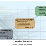
The chart shows Model Speed on the X-axis, where higher simulation speed is favored by software developers and speeds of hundreds of MIPS are now possible if you write a Loosely Timed (LT) model, shown in Green. To attain that high speed requires that the model be written at a high-level of abstraction, meaning that low-level details be omitted. Programmers benefit directly from Loosely Timed models because they can develop and debug their new apps, profile their software and determine if the architecture is compliant to specs.

In the bottom-left corner is the Grey box showing that Cycle Accurate (CA) models can be created that are faithful to the RTL timing as defined by the hardware engineer. Because the timing is accurate you can develop device drivers with a Cycle Accurate model, and also perform hardware/software co-verification, finding and fixing bugs before fabricating the SoC.

Instead of creating a third level of modeling as shown in Brown called Approximately Timed (AT), the approach taken by ARM and Carbon is to combine the benefits of both Loosely Timed and Cycle Accurate models.

Loosely Timed Models
An Architectural Envelope Model (AEM) is created first as an executable spec of the architecture. The AEM can be further refined to a specific CPU core using implementation specific details or adding optional features.

High simulation speed is gained by doing Code Translation (CT), a technique where code sequences for the specific CPU get translated to code sequences on your computer to be run natively. This CT approach runs much faster than previous approaches like interpreted Instruction Set Simulators. A typical 2GHz workstation could simulate the Android OS on a model of the ARM Cortex-A15 processor in about 50 to 100MIPS.

Cycle Accurate Models
The CA model has to create correct results for every cycle plus functionally correct results every cycle. This CA model can even be used as a replacement to RTL (Register Transfer Level) code, possibly requiring pin adaptors.

ARM IP also has CA models that were created automatically from RTL code using Carbon software, so you don’t have to do any modeling work, just use the CA models. On the other end of the speed spectrum ARM also provides Fast Models which can be interchanged with the CA models.

When you need to do some debugging, then use CA models. For pure speed, instead use the LT models.

Virtual Platform with Cycle Accurate and Loosely Timed Models
When you want to develop firmware it’s recommended to keep the processor and memory subsystem modeled as LT for speed, and then use CA models as needed. The limit to simulating with a combination of LT and CA models will be the CA model speed because of it’s higher detail.

A new technology called swapping even lets you start out with all LT models, gaining high speed, then at the time of interest swapping in some more detailed CA models to continue.

To do the model swapping requires creating a checkpoint of your system, so each of your models must support checkpoints.

Different Approaches
Here’s a quick comparison of what Carbon recommends versus other virtual prototype approaches:

[TABLE] style=”width: 500px”
|-
|
| Fast Simulation
| Best Accuracy
| Fast + Accurate
|-
| Carbon
| LT models
| CA models
| Swapping
|-
| Others
| LT models
| Emulator or FGPA Prototype
| – None –
|-

So other approaches give you either fast simulation or accuracy, however never at the same time. The downside of an emulator is the high cost, and the downside of an FPGA prototype is limited visibility to debug.

Swapping does have some downside, like cache contents are not saved, so stay tuned for more improvements ahead.

Summary
The approach of using both Loosely Timed and Cycle Accurate models together in a virtual prototype for ARM IP is compelling because of the 50-200 MIPS simulation speeds. This approach accelerates software debug, firmware development, architectural exploration, performance analysis and system debug.

Further Reading
10 page White Paper


Apple Makes More on iPhone Than Samsung on Everything

Apple Makes More on iPhone Than Samsung on Everything
by Paul McLellan on 01-25-2013 at 1:39 pm

Apple’s stock is down 10% after they announced “disappointing” results. They are only disappointing in the sense that some analysts expected even bigger profits. At $13.08 billion it is the largest quarterly profit for any corporation that is not in the oil business ever. According to wikipedia, even the oil companies only ever managed 3 quarters where they made a bigger profit.

Samsung announced its preliminary results too. Their profits were up 89% to $8.3B. Sales of the Galaxy S III reached 30 million units five months after it was introduced in May…nice, but Apple sold 48M iPhones (unfortunately analysts expected 50M) since iPhone5’s introduction in September, so in 3½ months. That’s twice the rate.

In fact Apple makes so much money on iPhone that its profits on iPhone alone are greater than Samsung’s profits overall. And Samsung are (by revenue) the largest electronics manufacturer in the world. Oh and they have a semiconductor division that must be doing pretty well since they make so many components for…Apple.

Perhaps the most amazing Apple number is that its operating expenses were just $3.2B last year. They took $3.2B and used it to make $40B in profit. Their gross margins are around 40% on everything they sell. They have fewer than 100,000 employees and half of those are in the Apple stores, the most profitable retail per square foot ever seen (more than Tiffany’s for example).

Of course Apple does face a problem. It is so large and so profitable that it is hard to keep growing profits fast, which is why the stock is down. Revenues were up by 18% last quarter compared to 2011. But Apple made over $40B in profit last year. To grow by 18% again means finding another $7.2B in profit. Apple’s net margins are roughly 25% so that means adding about $30B more in revenue. That is a lot. Intel’s annual revenues are $50B for example. The smartphone market and the tablet markets are for sure not saturated, but the steepest part of the growth curve may be over, especially at the premium end. In fact one of the worries that analysts have is that the iPad mini is cannibalizing sales of the iPad not-mini and, of course, delivers less profit per unit. If Apple, as predicted, releases an iPhone nano it will have the same problem. It will probably be a wild success but, at a lower price point, deliver less profit per unit.

All the numbers are not in yet for the entire mobile market, but it may well be the case that, once again, Apple and Samsung between them made more profit than the entire market, as has been the case for the last few quarters. All the other players aggregated together lost money. Not all of them, probably Lenovo, Sony and Huawei will be profitable at least. Even Nokia made money in its last quarter (if you lay off 20,000 employees you can get by with a lot less revenue). Google’s Motorola is still losing money though, and many of the other companies do not have enough volume to be able to make money.

Of course Apple may well find another entire product line. With Apple making over half its money on iPhone it is hard to remember that it is less than a decade since it was introduced (June 2007). The long-rumored Apple TV may turn out to be big…or not…or non-existent.

One of the unremarked stories, too, is the switch from WinTel to Mac. Go to any Starbucks and look around. Everyone has a Mac. No-one has a PC. The PC is still king inside corporations but outside, not so much. Go to any web company. Macs everywhere. Graphics, music…all Macs.


A Brief History of Sidense

A Brief History of Sidense
by Daniel Nenni on 01-24-2013 at 9:00 pm


Sidense Corp. is a leading developer of embedded non-volatile memory (NVM) intellectual property (IP) for the semiconductor IC market. The company is headquartered in Ottawa, Canada, and has a global presence with sales offices worldwide.

The company was founded in 2004 by CTO Wlodek Kurjanowicz, a MoSys fellow and co-founder of ATMOS Corporation. Wlodek saw a need in the market for a more area- and cost-efficient, and better performing NVM solution than provided by existing embedded NVM IP offerings or traditional EEPROM and flash. With this goal in mind, he developed the antifuse-based 1T-Fuse™ one-time programmable (OTP) bit cell, using a single-transistor split-channel architecture, for which Sidense has been granted several patents.

The 1T-OTP macros introduced definite advantages for chip developers by providing a small footprint, secure and reliable NVM solution using standard CMOS logic processes. Sidense quickly gained traction in the market, securing its first design wins for its SiPROM 1T-OTP macros by 2006 for code and encryption key storage in processor SoCs – the inherent security of the 1T-Fuse bit-cell and cost-effectiveness as a field-programmable solution being proven in the market.

By 2008 Sidensemarked its 50[SUP]th[/SUP] customer tapeout with 1T-OTP and the first customers in production using this technology. Additionally the early innovative work done by Sidense resulted in several prestigious awards, including a Red Herring Canada 2008 Top 50 Award, a Companies-to-Watch Award in the Deloitte Technology Fast 50 Awards in 2008, and inclusion in EE Times 60 Emerging Startups list for 2008. As the development and support team grew to support its success, the company moved into larger offices in Ottawa.

Since then,Sidense has broadened its product offering to address NVM needs in different applications across many technologies. As the 1T-Fuse technology provides a small footprint solution, it is compact enough to support field programming of code and data updates, emulating multi-time programmable memory. With fast access time and wide I/O bus configurations, code can often be run from OTP memory without copying to RAM, fitting well with ROM replacement and mobile SoC code-storage applications. To address other trimming and fuse-replacement applications, the company introduced the ULP 1T-OTP macros in 2010, providing ultra-low power operation, fast power-on read of bit settings and small footprints for very power-sensitive analog and mixed-signal designs.

Embedded 1T-OTP for Code Storage

Focusing on customer and foundry requirements for manufacturability and reliability, the company has developed strong relationships with the top-tier semiconductor foundries and key IDMs, working closely to put 1T-OTP products through their qualification programs. In addition to implementing 1T-OTP in leading-edge, small-geometry CMOS logic processes, Sidense has introduced products for high-voltage and power/BCD technologies. These support NVM needs in such applications as power management and analog devices for high reliability and “under the hood” 150°C operation for automotive and industrial subsystems.

The company has grown to support increasing demand for its 1T-OTP products and broad market adoption of the technology. Sidense 1T-OTP is now licensed to more than 100 customers worldwide, including many of the top fabless manufacturers and IDMs, and is on devices in production across all major semiconductor market segments.

A wide range of 1T-OTP macros are now available in many variants at process nodes from 180nm down to 28nm, and the technology has been successfully tested in 20nm. The company’s focus looking ahead is on maintaining a leadership position with NVM at advanced process nodes and solutions focused on customer requirements in the major market segments, including mobile and handheld devices, automotive, industrial control, consumer entertainment, and wired and wireless communications. Sidense will continue to work with its foundry and other partners to develop new products and product enhancements to meet the evolving needs of its customers as they take advantage of migration to the latest generation of advanced process nodes and of new market opportunities.