Bronco Webinar 800x100 1

How to manage decreasing by 70% a $5B IC business in less than 6 years? TI knows the answer…

How to manage decreasing by 70% a $5B IC business in less than 6 years? TI knows the answer…
by Eric Esteve on 01-24-2013 at 9:40 am

The Wireless Business Unit (WBU) from TI was created in the mid 90’s to structure the chip business in wireless handset made with customers like Nokia, Ericsson or Alcatel. I had a deep look at the WBU results: quickly growing from $1B in 2000 to reach about $5B in 2005… to finally decrease by 70%, down to $1.3B in 2012.

Let’s make it clear: TI is a great company, which has enabled the modern SC industry as we know it today, based on “Integrated” Circuit (invented by Jack Kilby in 1958). TI is also a company I had the great opportunity to work with, able to train a pure ASIC designer like me to a business-oriented engineer, allowing me to benefit from MBA level trainings, as well as exciting work environment – and great colleagues. Today, I will just use this market oriented education to try to understand what the mistake was. No doubt mistakes have been done, precisely understanding the nature of the mistake(s) just could help avoiding making it again.

In the early 90’s, TI top customer moved from IBM (DRAM and commodities for PC) to Ericsson, Cisco or Alcatel. If you prefer, the move was from the PC to the communication segment or from a commodity business (DRAM, TTL…) to the so-called Application Specific Product (ASIC, DSP…) business type. TI was leader in DSP, like TMS320C50 family, essential to support the new digital signal processing techniques used in modern communication. TI was lucky enough to have customers like Alcatel, able to precisely specify the ideal DSP core to support baseband processing of the emerging wireless (digital) standard, the GSM. TI management was cleaver enough to accept to develop the LEAD, a DSP core to be integrated into a chip using ASIC technology, along with a CPU core from a young UK based company, ARM Ltd…., into a single chip, that we know today under the “System-on-Chip”, this SoC being used to support the complexes GSM algorithms’ (baseband processing) and wireless handset related applications. Like for example to support this Ericsson handset model from 1998:

In 1995, all the pieces were already in place: Technology (ASIC), IP cores (LEAD DSP and ARM7 CPU) and customers: Ericsson, Nokia, Alcatel and more. By the way, at that time, TI Dallas based upper management was not aware that Nice (south of France) based European DSP marketing team, headed by Gilles Delfassy and counting Edgar Ausslander and Christian Dupont, had started deploying this wireless strategy! This team was cleaver enough to wait until the market clearly emerges, and the business figure to become significant, before to ask for massive funding. They literally behaved like they were managing a Start-up, except the start-up was nested in a $6B company!

President at Delfassy Consulting, Founder and GM (retired 2007) of Texas Instruments Wireless BusinessGilles Delfassy: President at Delfassy Consulting, Founder and GM (retired 2007) of Texas Instruments Wireless Business

Edgar Ausslander: VP, Qualcomm, Responsible for QMC (Qualcomm Mobile and Computing) product roadmap

Louis Tannyeres: CTO (TI Senior Fellow) at Texas Instruments

Remark: their respective titles are the currentLinkedIn title; a couple of years ago, Gilles Delfassy was CEO, Edgar Auslander VP Planning Strategy and Louis Tannyeres SoC Chief Architect, all of them with ST-Ericsson.

The WBU was officially created in 1998 and was weighting a couple of $100 million. The strategy was good, the market was exploding, the design team quickly growing, with people like Louis Tannyeres joining as technical guru (Louis is TI senior fellow), allowing to support as many customers as TI could eat, including Motorola (TI historical competitor) in 1999, it was not a surprise that WBU reach 1B$ mark in 2000. At that time, TI was offering a very complete solution: digital baseband modem and application processing, plus several companion chips (RF, power management, audio…) but let’s concentrate on the first mentioned. TI was the first company to introduce a Wireless dedicated SoC platform, OMAP, in 2002. Please note that this was possible because TI could offer both the digital baseband modem and the application processor, integrated into a single chip…

Again this was a winning strategy, explaining why WBU grew from $1B in 2000 up to $4.4B in 2005. In the meantime, CDMA had emerged and was competing with GSM, as precisely described in this brilliant post from Paul McLelan. Every company developing a CDMA compliant modem chip has to pay a license to Qualcomm, and Qualcomm was necessarily a competitor to this chip maker. Not a very comfortable position, but CDMA was opening most of the US based wireless market, so the choice was between getting almost no revenue in the US (and a few other countries)… or negotiating with Qualcomm. The below picture, showing how many CDMA royalties Samsung had to pay to Qualcomm during 1995-2005, clearly indicates that the CDMA royalty level is far to be negligible!

This 2005-2006 times was the apogee of TI WBU. In 2006, Qualcomm revenues from QCT (equivalent to WBU, chip business only, not integrating licenses) were $4.33B when TI WBU was above $5B. TI was already selling OMAP platform on the wireless market, when Gobi and Snapdragon were two years to be launched. TI’s position was still the leader, even if it was clear that Qualcomm was becoming stronger year after year. The only smartphone available on the market was from Nokia, and the iPhone was still not launched. Then, in 2007, two consecutive events happened: TI decided not to develop baseband modem any longer, and Gilles Delfassy retired…

If I remember well, the “official” reason to stop new modem development was because “digital baseband modem was becoming a commodity product”. Commodity means that the only differentiation can be done on the product price, on large production volume sales. Maybe Samsung, still fighting to launch an efficient 3G modem, would like to comment about the commodity nature of the digital baseband modem? In fact, the real reason was that TI was unable to release a 100% at spec, working 3G modem.

This sounds like in a tale from La Fontaine, “Le Renard et les Raisins”. In the tale, a fox is trying to catch grapes. Unfortunately, these grapes are located too high for him, so he fails to catch (and eat) these. Very disappointed, but pride, he says: ”Ils sont trop verts, et bon pour les goujats”, which means “these grapes are not ripen and good only for coarse person”. Just like TI upper management saying that “3G modem IC is a commodity market that we prefer not to attack”…

Moreover, even such a customer may hesitate before choosing TI when the competition (Qualcomm, Broadcom, STM) can propose to support a roadmap, where the next generation will be based on a cheaper solution: a single chip, integrating AP and Modem. Which is even more dramatic is that TI took this decision in 2007, if you remember it was precisely the year when Apple has launched the first iPhone, creating the smartphone market segment. The smartphone shipments have reached a record in 2012, with more than 700 million units being shipped. But TI has decided to concentrate on the Analog business, not on the wireless handset segment anymore. Who has said that Analog was a commodity business? I remember, it was during one of the training in marketing I had during my TI days…

By the way, any idea about TI WBU revenue in 2012? It was $1.36B, or 30% of 2006 revenue. But this trend could have been projected back in 2007, when TI has decided not to develop Digital Modem for the wireless market, wasting 10+ years R&D and business development effort.

From Eric Esteve from IPNEST


The Linley Microprocessor Conference: Weather Cloudy

The Linley Microprocessor Conference: Weather Cloudy
by Paul McLellan on 01-23-2013 at 7:51 pm

The Linley Group’s Microprocessor conference in Spring is focused on Datacenters now that cloud computing and massive internal datacenters has made them so important. The conference is on February 5th and 6th. It is free to qualified people such as network equipment vendors, network service providers and so on (which doesn’t include employees of semiconductor or EDA companies who have to pay).

The keynote on the first day at 9am is on Datacenter and Cloud Computing by Jag Bolaria and Bob Wheeler of the Linley Group.

On the second day, also at 9am, the keynote is Software Defined Networks
by Howie Xu who is VP of Engineering at Big Switch Networks.

At 2.25pm on the 6th is what looks like it will be an especially interesting session. The official topic is Designing Power-Efficient Serversbut unofficially (that is to say imho) it is really about whether ARM will make it in the server world or whether that will remain an Intel walled city. As will all the sessions, the presentations will be followed by a panel discussion. The three presenters and the titles of their talks are:

  • The Truth about ARM-based Servers; Performance and Power Measurements by Karl Freund, Vice President of Marketing, Calxeda
  • Architecting a Cloud Server for Evolving Data Center Workloads by Chris Bergen, Director of Technology, Applied Micro Circuits
  • Server Processor Landscape by Linley Gwennap, The Linley Group

One bit of bad news is that the first day of the conference coincides with the Common Platform Technology Forum. The good news is that the Linley conference has moved to the Hyatt hotel (it used to be in the Doubletree) and so it is possible to sort of attend at least some of both of them since CPTC is in the Santa Clara Convention Center attached to the hotel.

Details of the conference are here. For anyone trying to work out if they can see what they want at both the Common Platform Technology Forum and the Linley Data Center Conference, the CPTF detailed agenda is here. I, for one, will be back and forth between the two.


You may want to check that known-good RTL

You may want to check that known-good RTL
by Don Dingee on 01-23-2013 at 1:00 pm

In his blog Coding Horror, Jeff Atwood wrote: “Software developers tend to be software addicts who think their job is to write code. But it’s not. Their job is to solve problems.” Whether the tool is HTML, C, or RTL, the reality is we are now borrowing or buying more software IP than ever, and integrating it into more complex designs, and new issues are emerging.

Continue reading “You may want to check that known-good RTL”


Using IC Data Management Tools and Migrating Vendors

Using IC Data Management Tools and Migrating Vendors
by Daniel Payne on 01-23-2013 at 10:50 am

Non-volatile memory is used in a wide variety of consumer and industrial applications and comes in an array of architectures like Serial Flash and CBRAM (Conductive Bridging RAM). I caught up with Shane Hollmer by phone this week to gain some insight into a recent acquisition of Atmel’s serial flash components, and how that affected their EDA tool flow for IC data management.


Continue reading “Using IC Data Management Tools and Migrating Vendors”


Verdi: No Requiem for Openness

Verdi: No Requiem for Openness
by Paul McLellan on 01-22-2013 at 8:10 pm

I sat down last week for lunch with Michael Sanie. Mike and I go back a long way, working together at VLSI Technology (where his first job out of school was to take over the circuit extractor that I’d originally written) and then in strategic marketing at Cadence. Now Mike has marketing for (almost?) all of Synopsys’s verification products.

Of course, post Springsoft acquisition that includes Verdi. I’ve written about Verdi before, most recently when they announced Verdi[SUP]3[/SUP]and when they announced VIA, Verdi Interoperability Apps. Verdi is probably the industry’s most widely used debug system, widely used in verification groups. Historically it has been a very open system, not restricted to any one verification environment (since SpringSoft didn’t have their own simulators, emulators etc this wasn’t really an option anyway).

With Synopsys acquiring Springsoft there was a worry from industry and users as to whether Verdi would continue to be an open debug platform or would Synopsys limit the interfaces to only Synopsys tools and cut out, for example, interfaces to Cadence’s Palladium. This is especially important since the release of Verdi[SUP]3[/SUP] since much of what was new in that release was a much more open infrastructure:

  • new user-interface and personalization capabilities
  • open platform for interoperability and customization
  • new infrastructure for performance and capacity improvements

Well, Synopsys has no such plans to restrict Verdi to Synopsys’s own verification tools. It will continue with Verdi’s traditional stance of complete openness (FSDB, interfaces and the Verdi Interoperability Apps still at www.via-exchange.com). In fact Synopsys is going out of their way to communicate this to the industry even running an ad campaign since last November. All pervious user flows to use Verdi with simulators, emulators, formal verification tools, model checking engines, FPGA prototyping…all these will continue to be there.

Another interesting product that Synopsys acquired with Springsoft is Certitude (which I have also written about before). This is a tool for giving feedback on just how good (or not) your verification suite is. Unlike code coverage and other similar static techniques, Certitude works by injecting bugs into your design and then seeing just how many of them your verification flow manages to detect.

Of course, for reasonable sized designs it is never possible to exhaustively simulate or even formally verify the whole design, so it remains a judgement call whether “enough” testing has been done on the RTL. But Certitude gives an objective measure of stimulus and checker completeness to support this signoff decision, along with pointers to specific holes to accelerate the closure process by directing incremental efforts to the areas requiring additional attention.

Recently Synopsys hosted a webinar on Certitude which is available for download here.


How We Got Here…

How We Got Here…
by Paul McLellan on 01-22-2013 at 12:54 pm

Over at the GSA Forum website I have an article on the history of the semiconductor industry. It is actually based on a couple of brief history of semiconductor blogs (here and here) I published here on SemiWiki last year but edited down a lot and tightened up.

Since the start of the year seems to be the time for predictions, here are the last couple of paragraphs, which are a look to the future. No surprises here for anyone who has been reading my stuff, I’m not as optimistic as some people:Looking to the future, Moore’s law is under pressure. Not from a technical point of view; it is clear that it is possible to go on for many process nodes, but from an economic point of view: it is not clear that the cost to manufacture a million transistors is going to come down.

One major challenge is that for the foreseeable future, multiple masks are needed to manufacture some of the chip, pushing up costs. Extreme ultra-violet lithography (EUV) is a possible savior, but there are so many issues that it probably will not be ready until the end of the decade. Bigger 450mm (18-inch) wafers are another possible driver to bring down costs, but are also years away.

So it is possible that the exponential cost reduction that has driven electronics for decades is coming to an end. Electronics will still have more capability, but may not get cheaper and cheaper in the way that we have become accustomed.

The GSA Forum website is here. My article is here. You can download the entire December 2012 issue of GSA Forum here (pdf).


New PCI Express 3.0 Equalization Requirements

New PCI Express 3.0 Equalization Requirements
by Eric Esteve on 01-22-2013 at 9:18 am

PCI Express 3.0 increased the supported data rate to 8 Gbps, which effectively doubles the data rate supported by PCI Express 2.0. While the data rate was increased, no improvement was made to the channels. As such, an 8 Gbps channel in PCIe 3.0 experiences significantly more loss than one implemented in PCIe 2.0. To compensate for this increased loss, PCI Express 3.0 specifies enhanced equalization in the PHY with improved TX equalization, improved RX equalization, and equalization training.

It is critical that designers who plan to implement PCIe 3.0 understand these equalization changes and their impacts. After attending this webinar from Synopsys, registrants will understand:

  • Why improved levels of equalization are necessary at higher data rates
  • Types of equalization enhancements required for optimal performance at 8 Gbps
  • The difference between decision feedback equalization (DFE) and continuous time linear equalization (CTLE)
  • The need for equalization training and adaptability in PCIe 3.0
  • The importance of proven interoperability between the PHY and the controller

Who should attend:SoC designers and system architects. They may register here… do it quickly, as the webinar will be heeld on January 24 (this Thursday).

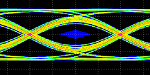
I remember, back in 2008, when Snowbush designers were implementing these advanced equalization techniques (DFE, CTLE), that one of the critical point was the number of “taps” in the equalization strategy: is two taps enough or should we implement three taps? I would certainly ask this question to Synopsys when attending this webinar! If you don’t know the mathematical (or Digital Signal Processing-DSP) principles of equalization and would like to learn, it will take you some brain gas, and time, my advice would be to find a good teacher. I was lucky enough 20 years ago to learn Equalization when working in a DSP oriented ASIC design team with DSP experts… it took me several 3 hours set to start (only start) understanding it! You can see one of the numerous steps on the above picture…

Coming back to Synopsys PCIe gen-3 PHY IP, not only the design is 100% compliant with PCI Express specification, but the test strategy is also very solid:
The test features include:

  • Unique built-in diagnostics enables visibility into link performance
  • Automatic Test Equipment (ATE) test vectors for complete, at-speed production testing
  • Built-in per channel BERTs

    • Flexible fixed and random pattern generation
    • Error counting on patterns or disparity
    • Digital phase or voltage margining (bathtub curves)
  • Built-in per channel non-destructive scopes: captures eye diagrams and coherently captures periodic signals in situ without disrupting link operation
  • Additional loopbacks:

    • Serial analog (for wafer probe)
    • Parallel Tx to Rx
  • Supports full analog ATE test on low cost digital tester using only pass/fail JTAG vectors

Presenters:


Rita Horner, Senior Technical Marketing Manager for Analog/Mixed Signal IP, Synopsys
Rita Horner has more than 20 years’ experience in mixed-signal circuit design, interconnect, test, and packaging of high-speed integrated circuits for consumer, computing, and high-end networking ASSP and ASIC products. As a technical and product marketing manager, she has experience in ASSP, ASIC and Fiber Optic products, focusing on High Speed Serial Interconnect. She participated and presented in multiple standards bodies including ANSI T11, IEEE 802.3, OIF, and SFF Multi Sourcing Agreements.


David Rennie, Senior Analog Design Engineer for Mixed-Signal Interface IP, Synopsys
David Rennie is a Senior Analog Design Engineer for Synopsys’ Mixed-Signal IP, developing next-generation high-speed PCIe and Ethernet SerDes technologies. David has authored and co-authored fifteen IEEE conference and journal papers and holds five granted and three pending patents. He has presented at several industry and IEEE conferences, and is an active member in the IEEE.

Eric Esteve from IPNEST


First Time, Every Time

First Time, Every Time
by SStalnaker on 01-21-2013 at 7:10 pm

While this iconic advertising phrase was first used to describe the ink reliability of a ballpoint pen, it perfectly summarizes the average consumer’s attitude toward automobile reliability as well. We don’t really care how it’s done, as long as everything in our car works first time, every time. Even when that includes heated car seats, remote engine controls, power windows and locks, satellite radio, wireless communications, automated traction sensing controls, and the myriad of other electronics-based features present in today’s cars and trucks.

These systems encounter demanding design constructs and operating conditions that can challenge manufacturers’ reliability and quality goals. Given this ever-present conflict between complexity and dependability, it’s no surprise that the automotive electronics industry is constantly looking for ways to enhance the design and verification of electronic components and systems to improve their dependability, operating efficiency, and functional lifespan. I recently looked at some of the challenges they face, specifically as they relate to circuit reliability verification, and some of the new techniques and tools that have been developed to address these needs.

Below is a brief excerpt from a recent article by Dina Medhat that discusses some of these design challenges, and the tools and techniques automotive designers are turning to for solutions.

Circuit Reliability Challenges for the Automotive Industry

In the automotive industry, reliability and high quality are key attributes for electronic automotive systems and controls. It is normal for automotive applications to face high operating voltages, and high electric fields between nets that can lead to oxide breakdown. Moreover, electrical fields can influence sensitive areas on the chip, because high-power areas are commonly located next to logic areas. Consequently, designers must deal with metal spacing design rules that are dependent on voltage drop. Trying to implement such rules in the entire design flow, starting from layout routing implementation through design rule checking (DRC), is too conservative, as well as inefficient, due to lack of voltage information on nets (both in schematic and layout). Trying to achieving this goal with traditional exhaustive dynamic simulation is simply not practical, due to the turnaround time involved, and, if the design is very large, it may not even be possible to simulate it in its entirety.

New circuit reliability verification tools such as Calibre® PERC™ provide a voltage propagation functionality that can help perform voltage-dependent layout checks very efficiently while also delivering rapid turnaround, even on full-chip designs. In addition, they provide designers with unified access to all the types of design data (physical, logical, electrical) in a single environment to enable the evaluation of topological constraints within the context of physical requirements.

For a more detailed explanation of these issues, along with some examples of voltage-dependent design rule checking, negative voltage checking, and reverse current processing, read the entire article.


Double Patterning for IC Design, Extraction and Signoff

Double Patterning for IC Design, Extraction and Signoff
by Daniel Payne on 01-21-2013 at 3:27 pm

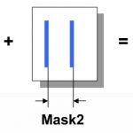
TSMC and Synopsys hosted a webinar in December on this topic of double patterning and how it impacts the IC extraction flow. The 20nm process node has IC layout geometries so closely spaced that the traditional optical-based lithography cannot be used, instead lower layers like Poly and Metal 1 require a new approach of using two masks per layer. Using Extreme UltraViolet (EUV) with it’s shorter wavelength could get us back to 1 mask per layout layer, however EUV is not ready for production use quite yet.

Continue reading “Double Patterning for IC Design, Extraction and Signoff”


FD-SOI is Worth More Than Two Cores

FD-SOI is Worth More Than Two Cores
by Paul McLellan on 01-20-2013 at 10:00 pm

This is the second blog entry about an ST Ericsson white-paper on multiprocessors in mobile. The first part was here.

The first part of the white-paper basically shows that for mobile the optimal number of cores is two. It is much better to use process technology (and good EDA) to run the processor at higher frequency rather than add additional cores.

ST Ericsson, as belies its name, is partially owned by ST (although they are trying to get rid of it, as are Ericsson. Dan Nenni has the same problem with his kids, they just hang around and cost a lot of money). Unlike everyone else who has decided the future is FinFET, ST has decided to go with FD-SOI (Chenming Hu was better at naming transistors than whoever came up with that mouthful). FD stands for fully-depleted, meaning that the channel area under the gate is not doped at all. SOI stands for silicon-on-insulator since the base wafer is an insulator. One of the advantages that FD-SOI has over FinFET is that it is essentially a planar process very similar to all existing processes and so can be build using very mature technology with fewer process steps than “other” processes (by which I read FinFET).


Compared to a bulk transistor, the advantages of FD-SOI are that it is faster and lower power. In a given technology node the channel is shorter and it is fully-depleted, both result in up to 35% higher operating frequency for the same power at high voltage and up to 100% faster at low voltage. The fully depleted channel removes drain-induced parasitic effects and has better confinement of carriers from source to drain, a thicker gate dielectric reducing leakage and so on. The result is power reductions of 35% at high performance and 50% at low operating points.

So for a processor, obviously, it can be run at a higher frequency for the same voltage/power or run at the same frequency without consuming so much power. The maximum achievable frequency is higher. And the process can operate at lower voltages with reasonably high frequencies (such as 1GHz at 0.65V).

This 35% increase in efficiency a high frequencies is more than enough for FD-SOI dual processors to outperform slower bulk quad-processors due to the limited software scalability. It also can obviate the need to optimize power by using heterogeneous big.LITTLE type architectures which requires complex hardware and sophisticated control mechanisms that are not yet mature.

ST Ericsson was an early adopter of dual processors but have resisted moving to quad core for all the reasons in these papers. However, this is probably academic. ST Ericsson has struggled to find major customers (partially because Apple and Samsung take most of the market and roll their own chips, and their biggest customer was Nokia who switched to Microsoft WP which only runs on Qualcomm chips). ST and Ericsson both have announced that they want to “explore strategic options” for STE (aka find a buyer) but it may end up that the company ends up simply being shut down. The group that I worked with at VSLI Technology in the 1990s, ended up inside NXP and was then folded into ST Ericsson. I notice on their blog entries the names of some people that used to work for me.

Download the white-paper here.