Bronco Webinar 800x100 1

Wall Street Does NOT Know Semiconductors!

Wall Street Does NOT Know Semiconductors!
by Daniel Nenni on 01-20-2013 at 6:00 pm

In my never ending quest to promote the fabless semiconductor ecosystem I cannot pass up a discouraging word about one of the oldest financial services companies. You can consult with me for $300 per hour to answer your questions about the semiconductor industry on the phone or you can buy me lunch and get it in person (lunch will probably cost you more). The people who hire me are usually financial types (hedge fund managers etc…) but I also get called by semiconductor companies for market strategies and such. SoCs are a popular topic now and things get busy when quarterly results come in for TSMC, Intel, and the fabless guys in the mobile market segment. The fun part is taking apart analyst reports like the recent one from Morgan Stanley about TSMC.

Since its founding in 1935, Morgan Stanley and its people have helped redefine the meaning of financial services. The firm has continually broken new ground in advising our clients on strategic transactions, in pioneering the global expansion of finance and capital markets, and in providing new opportunities for individual and institutional investors. Click below to see a timeline of Morgan Stanley’s growth, which parallels the history of modern finance.

To start, look at the Morgan Stanley Wikipedia page which lists controversies and lawsuits with fines in the hundreds of millions of dollars.

TSMC released Q4 2012 numbers during last week’s conference call. You can read the Seeking Alpha transcript HERE. I’m a big fan of the Seeking Alpha transcripts, reading is much better than listening, unfortunately the Seeking Alpha analysts don’t know semiconductor either but more on that later.

Per Morgan Stanley:

[LIST=1]

  • 28nm is surprising on the upside (DUH)
  • 28nm Margins above expectations (DUH)
  • 20nm node to be bigger than 28nm (WRONG)
  • TSMC 6.5% Q1 revenue drop (WRONG)

    Disclaimer: This information came from a phone call so it may not be 100% accurate but it has been repeated by other analysts so they are valid discussion points.

    Morgan Stanley and others were surprised at the TSMC Q4 financial numbers which they should not have been. As I blogged before, 28nm will be the most successful node we have seen in a long time (in all regards) and TSMC owns it, thus the high margins. To be fair, TSMC warned that Q4 could be soft but I blogged otherwise. TSMC is a conservative company and can certainly play the Wall Street game. On the other hand, I would rather see ACCURATE forecasts from analysts so we can do business without shortages, layoffs, and the other things that go along with bad business decisions.

    In what way will 20nm be bigger than 28nm? Compare the value proposition of 28nm and 40nm versus 20nm and 28nm in regards to price, performance, and power consumption. The value proposition of 20nm is less than half of 28nm meaning some companies will do limited tape-outs at 20nm, some are even skipping 20nm completely in favor of 14nm FinFETs which should ramp shortly after 20nm. Samsung, GLOBALFOUNDRIES, and TSMC will all use Gate-Last HKMG and have 20nm production simultaneously so heated competition will be a factor. TSMC has the advantage of being on their second generation of the Gate-Last HKMG experience since Samsung and GLOBALFOUNDRIES used Gate-First at 28nm which did not yield as well. Samsung has the “Brute Force” 20nm advantage with what seems like unlimited resources and fab capacity. Samsung is also an IDM with internal SoC/VLSI design experience. GLOBALFOUNDRIES has the advantage of being the designated second source foundry by companies like Qualcomm and other big fabless companies that see Samsung as a ruthless competitor. The GLOBAFOUNDRIES New York fab is 20nm so customers can keep their IP protected under American law.

    Bottom line: 20nm is a completely different game than 28nm so any comparison will be much more complicated, be very careful who you listen to, my opinion.

    Q1 will be like Q4, underestimated, but that is all part of the Wall Street game. There is no stopping the mobile market, 28nm owns mobile, TSMC owns 28nm, simple as that. Seeking Alpha is still perpetuating the Apple at TSMC 28nm misinformation and, in general, I’m not impressed at all with their semiconductor coverage. If you read them do a quick author look up on LinkedIn. If they don’t have a profile there is probably a good reason for it. If they do, look for at least some semiconductor experience before investing your hard earned money their way.

    Also read: TSMC Apple Rumors Debunked!

  • Mobile SoCs: Two Cores are Better Than Four?

    Mobile SoCs: Two Cores are Better Than Four?
    by Paul McLellan on 01-20-2013 at 8:00 am

    I came across an interesting white-paper from ST Ericsson on two topics: multi-processors in mobile platforms and FD-SOI. FD-SOI is the ST Microelectronics alternative to FinFETs for 20nm and below. It stands for Fully-Depeleted Silicon-on-Insulator. But I’m going to save that part of the white-paper for another blog entry and focus on the mobile stuff here. By the end of this blog entry you will see why these two seemingly disconnected topics are in a single white paper.

    Multi-core originally was driven by the realization in the PC market by Intel that the power density of their processors was going to surpass that of the core of a nuclear reactor if they just kept upping the clock rate. Instead, increased computing power would have to be delivered not by a single core with more performance but by multiple cores on the same die.

    Initially this worked well since it was not hard to make good use of dual cores, one doing compute intensive stuff and one being responsive. But more cores turned out to be really hard to make use of (not a surprise to software type like me since making a big computer out of lots of little cheap ones has been a major area of research for many decades). Ten years later, most software including games, office productivity, multimedia playback, web browsing etc only make use of two cores. Just a few applications such as image and video processing have very easily partitioned algorithms that can make use of almost arbitrary numbers of cores.

    In mobile the multi-core change has come faster since the same power considerations are more urgent. The cliff was not that people couldn’t have a nuclear reactor in their pocket but that pushing the clock rate up too high killed battery life and so multi-core was a way of getting that back up again.


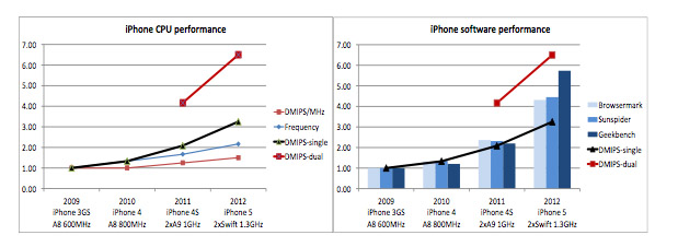
    But look as a close reading of the above graphs shows, single core performance isn’t, in fact, saturated at all and there is still strong acceleration. This is totally different from PCs which were clearly saturated very early. But, as for the PC, software only scales with single processor performance and less than proportionally (or, depressingly, not at all) for multiprocessors.

    So why have mobile platforms jumped into multi-core well before reaching saturation on the first core. One is that it could piggy-back on existing experience since it was already known that dual cores could be exploited well by operating systems and the fundamental technologies such as cache-coherence (and how to build them on silicon) were well understood. And the other is aggressive marketing (“mine’s bigger than yours”).

    What is unclear is why the major platforms have gone to 4 cores (or 8 the way Samsung counts) since the PC experience already shows that more than two processors is useless for most things (and people aren’t running photoshop on their phones). It turns out that there are no strong technical reasons, it seems to be entirely down to marketing since the number of processors is used for differentiation, even for the end-user (who, generally, wouldn’t know what a core was if you asked them, is it something to do with the center of the Apple?).


    For web browsing, especially with HTML5 rich content, processing speed is often the critical path rather than the network bandwidth (my LTE iPad downloads faster than my Mac iBook since LTE is faster than my wireless router). You can see from the above picture that going to dual core gets 30% speedup going from single to dual core, but 0-11% from dual to quad.

    On the other hand, frequency improvements always pay off. 1.4GHz dual core beats 1.2GHz quad core. In all the experiments STE have done, the results are the same. No benefit in going from dual core to quad core and 15-20% faster dual core always beating slower quad core.

    What this means is that increasing the frequency of the processor at constant power is more important than adding cores. This is where the FD-SOI part comes into play. Using process technology to get the frequency up 15% is better than adding cores beyond two.

    Download the white paper here.

    Also read: FD-SOI worth more than two cores


    What did CES 2013 mean for #SemiEDA?

    What did CES 2013 mean for #SemiEDA?
    by Don Dingee on 01-18-2013 at 4:55 pm

    CES is the preeminent gadget show, and in the LVCC South Hall a wave has been building for some time. It’s now the place where chipsets are introduced, and this year saw a wide range of introductions from Atmel, Bosch, Broadcom, Intel (OK, they’re still in Central Hall), InvenSense, Marvell, NVIDIA, Qualcomm, Samsung, ST-Ericsson, Tensilica, TI, ViXS, and more.

    Continue reading “What did CES 2013 mean for #SemiEDA?”


    Yawn… New EDA Leader Results Are Coming

    Yawn… New EDA Leader Results Are Coming
    by Randy Smith on 01-18-2013 at 4:00 pm

    We will soon start to see the quarterly financial reporting installments of the “Big 3” public EDA companies. I predict they will be as boring as usual. I am not sure if I would want it any differently though.

    Back in the 90s there were times when it was truly interesting to wait to see what Cadence, Mentor, or later Synopsys, might announce. I still have my brass-plated letter opener which Cadence gave to every employee in September 1990 when Cadence moved to the NYSE. Heck I even was excited to see the SVR (Silicon Valley Research, aka Silvar-Lisco) announcements. It was exciting to follow the industry then.

    So what changed? The biggest change in the past 20 years is the EDA revenue model. Instead of primarily selling perpetual licenses and annual maintenance, EDA vendors sell time-based licenses (TBLs) with bundled maintenance. For the customers, this somewhat lessened the gamesmanship as to what enhancements they got for free, and what constituted a new product for which they would have to pay more money. But the financial community loved it since it forced a smoothing out of revenue. A 3-year license is now recognized ‘ratably’ – 1/36 of the purchase price is counted as revenue each month. Under the old perpetual licenses all of the revenue was recognized with the booking.

    The effect of this change is fairly dramatic. If all the revenues were to be coming in on 3-year TBLs, then each quarter more than 90% of the company’s revenue is already made on the first day of the quarter. This is why all the analysts estimates are so close to each other and the announced number, too. How hard can it be?

    Table 1. Analyst Estimates for Q4-CY-2012

    How much do the analysts like predictability? Well, it was rumored that Cadence’s Executive VP of Sales Mike Schuh (now a General Partner at Foundation Capital), who lead Cadence’s sales team during its most explosive growth period, was forced out of Cadence after making his numbers yet again because a high percentage of the deals that actually closed that quarter were not in the forecast. So, despite always driving sales higher, Mike was seen as too unpredictable. [As an aside, I learned a tremendous amount watching Mike in sales situations – he was a brilliant salesman.]

    So where has this predictability gotten the big EDA companies? Well first, they didn’t really make a quick switch to this model. Some of them cheated in the eyes of the financial community. They sold their deals to banks so they could pull all of the revenue forward. They did “respins” of deals before they would expire making it more difficult to properly estimate their effect on revenue over time. But, over the past few years it has all seemingly been cleaned up. So thanks to Lip-Bu, Aart, and Wally for giving us credibility with Wall Street. I am still waiting for the other effect that should have happened…

    With a much more predictable revenue stream, I would have also expected it to be easier to plan an R&D investment stream, too. I expected that finally the Big 3 would come out with homegrown products that could redefine markets and upset the balance of power. That has not happened. Despite the declining number of EDA start-ups we are still not seeing any ground-shaking new products from the Big 3 EDA vendors. More about that in a later blog.

    There is yet another way this model might change. We might see more moves into the EDA space from adjacent spaces. Recently, not all EDA acquirers have been the traditional EDA vendors. That might shake things up a bit, too.

    Note: I run an executive consulting business. A list of my past and present clients can be found on my website, www.randysan.com.


    Oasys Has a New CEO

    Oasys Has a New CEO
    by Paul McLellan on 01-18-2013 at 2:21 pm

    Scott Seaton is the new CEO of Oasys Design Systems. Paul van Besouw, the CEO since the company’s founding, becomes the CTO. I met Scott last year when I was doing some consulting work for Carbon Design where he was VP of sales (the new VP sales at Carbon is Hal Conklin, by the way).

    I talked to Scott about why he had joined Oasys. After all, when you take on a CEO (or any senior position) in an early-stage company, the most important thing is whether you think that the company is going to be successful.

    He believes that in RealTime Designer and RealTime Explorer that Oasys has breakthrough technology. When he talks to customers, they tell him that they have reduced their time to market by an average of 2 months compared to their previous methodology.

    RTL designers need to get physical feedback. If they don’t use RealTime then the only way to do this is using the full implementation flow that typically takes 2-3 days. Oasys is at least 10 times faster than this. Further, since there is a single tool with a unified database, it is easy to highlight problems (such as timing constraint violations) and tie them back to the correct line of RTL. One customer told Scott that the last timing problem they tried to correct took them 6 hours just to find the correct bit of RTL. Cross-probing in RealTime takes a minute.

    Oasys recently introduced RealTime Explorer to address this issue whereby RTL designers either don’t get any physical feedback (in which case their timing numbers are pretty much meaningless) or where it is extremely cumbersome to get the data. This is especially critical with geographically remote RTL development groups who may not have any access to the physical tools or, indeed, the expertise to run them if they did. Up to now, other vendors have offered either estimation tools or else taken synthesis engines and de-tuned them to gain speed while sacrificing quality-of-results (QoR) and thus correlation. Customers tell Scott that neither of these approaches address their needs. By definition, RTL engineers that are trying to push the boundaries of performance don’t have much margin for error. And in advanced nodes like 28nm, everyone is trying to push the boundaries of performance otherwise why bother.

    Ultimately, none of this matters unless the customers are deriving real value. On every metric, Oasys is gaining momentum. Sales were up in 2012 by 114% over 2011 and they finished off in Q4 being cash-flow positive. Customers include 5 of the top 10 semiconductor companies, many using RealTime for 28nm tapeouts and some qualifying RealTime for production use at 20nm and 14nm nodes. All of them want to use RealTime for both RTL exploration and for implementation.


    Buying DDRn Controller IP AND Memory Model to the same IP vendor gives real TTM advantage

    Buying DDRn Controller IP AND Memory Model to the same IP vendor gives real TTM advantage
    by Eric Esteve on 01-17-2013 at 10:52 am

    We all know the concept of “one stop shop”, becoming popular in the Design IP market. The topic we will address today is NOT the “one stop shop”, even if it looks similar, but rather that we could call “consistent design flow”.

    What does that means? Simply that, if your SoC design is integrating a DDRn (LPDDR2, DDR3 or even DDR4, let’s say DDR3 in this case) Memory Controller, you will have to run functional simulations of your SoC behavior, being as close as possible of the real life, then these simulations should integrate accurate model of the DDR3 memory chip. The easiest and safest path is to acquire this model. Denali has been started in the mid 90’s with this primary charter, develop and sale Memory Models. Nobody ignore that Denali has been acquired in 2010 by cadence (for a record $315M, or about 7X the 2009 company revenue!), and that Denali’s port-folio was based on: Verification IP (for Interface IP like PCIe, USB and so on), DDRn Memory Controller IP and… the Memory Models.

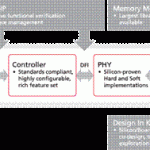
    Cadence has acquired Denali to reinforce the Verification IP port-folio (and buy VIP market share…) and to add the very successful DDRn Memory Controller IP to the existing IP business, as well as the Memory Model business, where Denali was almost in monopoly position. The above picture clearly shows that I mean by “Consistent Design Flow”: PHY and the Controller (or “Integrated”) IP that could be interfaced with Memory Model, the behavior of the SoC interacting with external DDR3 being validated by using Verification IP, in a specific simulator (that Cadence can also offer, but this is not necessarily part of the “Consistent Flow”).

    Within this Consistent Flow, we can find the DDRn Memory Controller “Integrated” IP. In this case, Integrated means that Cadence can provide both the PHY and the Controller IP. The Controller IP is 100% digital design, supporting the industry standard DFI PHY interface, when the PHY can be… either mixed signal Hard IP, either a soft IP. In fact, when Denali was providing DDRn Controller, the company was only proposing internally designed soft PHY, or Hard PHY from partners like Analog Bits or MoSys. Cadence has addressed this weakness after Denali acquisition and SoC design integrators can rely on Integrated solution (100% supported by internally designed pieces).

    But designers still have the choice between using Hard PHY (see above picture) or Soft PHY, as legacy customers used to do. What’s the difference between Hard and Soft PHY? Probably a different pricing, but Cadence promotes the Hard PHY as being a TTM accelerator, when the Soft PHY offers higher flexibility as we can see on the picture below. Just a remark: if you prefer the higher flexibility of the Soft PHY, not impacting the chip floor-planning as would do a hard block, you may spend longer to meet the DDRn PHY timing constraints. If you consider that the DDRn frequency will go higher with new generation adoption, you quickly realize that the trend will be to use integrated solution based on Hard PHY in the future…

    In fact, Cadence is going even further and offers a “System Integration Kit”, ensuring optimal system integration and eliminating overdesign. The idea is to propose an integrated silicon-package-board co-design environment, with IBIS models for DDRn PHY, reference implementations and diagnostics and analysis tools. Once again, the benefits will be accounted in TTM acceleration, as the solution allow to:

    • Enable topology modeling ahead of committing to a final implementation
    • Identifies SI issues early in the design process where they can be address at significantly reduced cost
    • Eliminates the need to overdesign saving significant amounts of effort and cost
    • Allows system design to begin much earlier than traditionally possible

    All of the above represent a significant investment for an EDA/IP vendor! The differentiation is offering clear benefits for the customer, especially in term of TTM acceleration, but does the DDRn memory controller IP represent a significant market segment, offering large enough ROI to Cadence?

    The answer is: we don’t know! I should say, we don’t know officially Cadence’s revenue or market share in the DDRn memory controller IP segment. IPNEST has made an evaluation of this segment business size, including Denali (then Cadence) for 2005-2011, as we can see on the picture below, but Cadence’s revenue could be lower… but my personal opinion is that it is even higher!

    By Eric Esteve from IPNEST – “Interface IP Survey 2005-2011 – Forecast 2012-2016” Table of Content available here

    As a bonus, two very relevant comments from a previous post about DDRn memory controller, if you have missed it:

    It’s interesting that your list of IP is mostly serial interfaces, DDRn seems to be a hold-out as a parallel bus. Given that the increasing number of cores causes more bus contention (with a shared parallel bus), is there much future in DDRn?

    04-14-2011 By Simguru

    I am not up to speed on all of the different interface stds. Others please correct me if I’m wrong.

    DDR is the fastest mechanism to transfer data to/from memory. Using both the positive and negative edges of a clock therefore decreasing clock speeds by 50% for the same data transfer rate. DDR does require PHYs like the other standards but I do not think this std has long cable lengths such as PCI Express, Xaui, USB, SATA, etc that must be met.

    DDR (3 and 4) can transfer up to ~2700-3200 MB/s (not bits) while SATA3 is 600MB/s, HDMI is 10Gb/s or 1.25GB/s which makes sense to meet audio/video standards, USB 2.0 is in 30-60MB/s (actual vs. max), etc.

    DDR can have a long future by wider word widths, faster clock rates, etc. I doubt for CPU/Memory interfacing, a serial std will replace it but stranger things could happen. Eric might have some research on this topic.

    I will also bet that many handheld device that could be plugged and benefit from DDR for higher transfer rates are not willing to pay royaltes for this functionality (DDR patent). The other standards are cheaper to embed (lower or non-existent royalties).

    my 2 cents.

    04-15-2011 By BillM


    Fixing Double-patterning Errors at 20nm

    Fixing Double-patterning Errors at 20nm
    by Paul McLellan on 01-16-2013 at 10:54 pm

    David Avercrombie of Mentor won the award for the best tutorial at the 2012 TSMC OIP for his presentation, along with Peter Hsu of TSMC, on Finding and Fixing Double Patterning Errors in 20nm. The whole presentation along with the slides is now available online here. The first part of the presentation is an introduction to double patterning but I’m going to assume everyone already has that background information. If not, look at my earlier blog here.


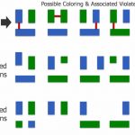
    The most common double patterning error is what is called an odd-cycle path. This is when an odd number of polygons are arranged so that there are minimum spacing (or technically spacing that are close enough to require the polygons to be on separate colored masks) between them in a loop. The simplest case is shown above where there are three polygons, and each has to be a different color from the other two, which is obviously impossible with only two colors to go around. It is worth emphasizing that there isn’t just a single spacing that is in violation, or a particular coloring that is in violation. It is impossible to correctly color the polygons. Instead of giving a spurious coloring and highlighting one of the violations as being “the” error, the violation is indicated by a square (or more complex polygon for more complex violations) that shows which are the polygons in the cycle (as in the above picture). The violation can be fixed by either increasing a spacing so as to break the cycle, or by removing a polygon completely, either breaking the cycle or making the cycle even (which is not a problem since it can be colored).


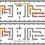
    One problem is that moving a polygon to fix one odd cycle can often cause the whack-a-mole effect whereby a new odd cycle gets created as in the above examples. This can obviously be frustrating, to say the least.


    David’s rules of thumb for not getting into endless odd-cycle purgatory is:

    • Move single edges as opposed to entire polygons when possible. This minimizes the chance of introducing unexpected new errors.
    • Remove (or split) polygons. Again, this is less likely to produce new errors.


    The rules are not foolproof however. One complication is that fixing one odd cycle path might have the effect of changing a nearby even cycle path (and therefore not a problem) into an odd cycle path and so creating a new violation, as in the two examples above. Mentor’s Calibre has some (apparently patented) technology for highlighting warnings to show where nearby paths intersect with error paths and so, at the very least, care must be taken. Watch the webinar for details.


    One final problem occurs with anchor paths, also known as pre-coloring. It is possible for the designer to select explicitly which of the two masks certain polygons must appear on. For example, the power and ground nets might be selected as going on the same mask to ensure that variation between the two nets is minimized. Of course, give a designer manual control and there is plenty of scope to get it wrong and create odd cycle paths between similarly colored polygons (or even cycle paths between different colored polygons) both of which make the design uncolorable. The fixes are mostly similar to any other odd cycle path, although there is another potential option which is to reduce the amount of pre-coloring or change the pre-coloring to colorable overall.

    Of course real layout may have both odd path violations and anchor path violations all mixed up together in the same part of the design. David’s advice is to attack the odd cycle path violations first since that often fixes some of the anchor path violations in any case. Then worry about anchor path violations.

    View the webinar here.


    Mentor @ the TSMC Open Innovation Platform Forum

    Mentor @ the TSMC Open Innovation Platform Forum
    by glforte on 01-16-2013 at 6:16 pm

    At TSMC’s Open Innovation Platform (OIP) Ecosystem Forum, Mentor made technical presentations on four different topics, two of them co-presented with TSMC and LSI Corporation. Those presentations are described below with links to downloadable pdf presentation files.

    Finding and Fixing Double Patterning Errors in 20nm Design

    David also won the Customer’s Choice award (selected by attendee vote) for his presentation on Finding and Fixing Double Patterning Errors in 20nm Designs at TSMC’s Open Innovation Platform ecosystem event. In this presentation, David describes the new constraints that double patterning brings to the 20nm node, and how IC designers can deal with DP related design rule violations. View presentation…

    A Platform for TSMC’s CoWoS 3DIC Reference Flow

    The first phase of 3DIC adoption will be based on silicon interposers. Designing multi-die systems using this technology introduces new challenges for the EDA design flow. At the TSMC OIP event, Mentor described solutions for 3DIC design specifically tailored to TSMC manufacturing processes.View presentation

    Automated Approach for Waiving Physical Verification Errors in IP

    Redundantly reviewing recurring errors during custom and third-party IP integration can slow down SoC verification. An automated waiver management methodology enables design and verification teams to specify and process a variety of design rule waivers, reducing debugging time and improving SoC results. Mentor and LSI recently described the use of this technology at the TSMC OIP event. View presentation

    Improving IC Design for Reliability

    Verification of 20nm designs is expected to bring significant challenges. A robust verification methodology that addresses circuit reliability is increasingly difficult. At 20nm, new devices that incorporate thin oxides are less robust and more subject to electrical overstress (EOS) failures. The increased use of mixed-signal and multi-voltage design techniques also increases the likelihood that transistors could be implemented in an incorrect voltage domain. At TSMC’s recent OIP event, Mentor showed techniques to prevent long term electrical failure using new tools to validate ESD structures, protect against EOS, manage multiple power domains, and carefully balance sensitive analog circuits. View presentation


    A Brief History of Apache Design

    A Brief History of Apache Design
    by Daniel Nenni on 01-16-2013 at 3:00 pm

    Apache Design Solutions was founded in 2001 by Andrew Yang and three researchers from HP Labs (Norman Chang, Shen Lin, Weize Xie). They realized that engineers striving to meet the goal of increased device miniaturization, as defined by Moore’s Law, would eventually hit stumbling blocks in their progress. The founding team believed that success in the end would depend on how well chip designers can manage the power consumption, power delivery and power density of their designs. They also believed that how well engineers navigated the fragmented, silo-based electronic design eco-system would help them achieve competitive differentiation and cost reduction for their end-products. The team realized that engineers use various architectural and circuit techniques, including reducing voltage supply, to control power consumed by smartphones, tablets and hand-held devices. But these techniques made circuits more vulnerable to fluctuations and anomalies, either when manufactured or operated.

    Before the release of Apache’s first flagship product RedHawk™ in 2003, chip designers relied on approximations, and ‘DC’ (or static) analysis methods, that are insufficient for predicting fluctuations coming from the interaction of the chip with its package and board. Apache’s RedHawk provided the industry with its first ‘dynamic’ power noise simulation technology, allowing chip designers to simulate their entire design, along with the package and board, and predict operation prior to manufacturing the parts. RedHawk introduced the industry to several key technologies that have become increasingly relevant, and are still unmatched over ten years later. These technologies include: (a) extraction of inductance for on-chip power/ground interconnects, in addition to their resistive and capacitive components, (b) linear model creation of on-chip MOSFET devices through the use of Apache Power Models, (c) automatic generation of on-chip vectors using a VectorLess™ approach, and (d) simultaneous analysis of multiple voltage domains handling billion+ node matrices, and considering various operating modes on the chip such as power up, power down, etc. In its debut year, RedHawk was presented with EDN Magazine’s Innovation of the Year Award (2003).

    RedHawk’s first-in-class technologies, built on best-in-class extraction and solver engines, has led to its adoption as the ‘sign-off’ solution of choice by electronic system designers around the world for power noise simulation and design optimization. The release of RedHawk was followed by the introduction of Totem™, meeting the distinct needs of analog, IP, memory, and custom circuit design engineers for power noise and reliability analysis.


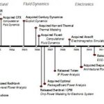
    Figure1: ANSYS-Apache products / company timelines.

    The introduction of the Chip Power Model (CPM™) technology and Sentinel™ product family in 2006, were seminal events in Apache’s history. For the first time, chip designers could create compact Spice-compatible models of their chips that preserved the time and frequency domain electrical characteristics of the chip layout. This model soon became the ‘currency’ for the exchange of power data enabling chip-aware package and system analysis. For its industry contribution, Apache’s CPM was presented with EDN Magazine’s Innovation of the Year Award (2006).


    Figure2: The growing gap between power consumption in electronic systems
    and the maximum allowed power budget.

    The success of smart hand-held devices depended on how efficiently designers could squeeze increasing functionality within much smaller form factors, while managing to meet the end device’s power budget. Apache’s acquisition of Sequence Design in 2009, and the introduction of the PowerArtist™ platform, addressed chip designers growing need to simulate designs very early during the design phase, when architectural definitions are created using register transfer language (RTL) descriptions. PowerArtist enables accurate and predictive RTL-based power analysis and helps identify power bugs and cases of wasted power consumption in the design. This simulation driven design-for-power methodology allows engineers to address the growing gap between device power consumption and the maximum allowed power in end electronics systems.


    Figure3: Increasing divergence between current flowing in wires versus their ability to handle such current levels.

    Increasing functionality requirements in smaller form factors have accelerated the adoption and use of advanced technology nodes such as 28-nanometer (nm) and below. The logic operations performed in a chip result in a flow of current in various inter-connects on the chip. But the wires and vias fabricated using advanced technology nodes cannot sustain increased current levels, and are at risk for field failures. Additionally, MOS devices and on-chip interconnects are increasingly susceptible to failures from high levels of current flow, resulting from an electro-static discharge (ESD) event. To address this growing design challenge, Apache introduced PathFinder™, the industry’s first full-chip level, package-aware ESD integrity simulation and analysis platform. PathFinder enables designers to predict and address ESD induced failure they would not be able to identify otherwise, until very late in the product design cycle. Apache’s PathFinder was also presented with EDN Magazine’s Innovation of the Year Award (2010).


    Figure4: The ANSYS-Apache simulation ecosystem brings semiconductor foundry, IP providers, SoC design houses, package vendors, and system integrators together.

    Apache’s innovative product platforms solve specific analysis needs and enable a simulation environment that brings together disparate design teams such as automotive or communications system companies and their IC suppliers, or IC design firms and their foundry or ASIC manufacturing partners.

    Apache’s revenue increased 3X from 2006 to 2010, underscoring the strong adoption of its products and technologies by semiconductor and system design companies worldwide. Apache’s achievements were recognized by being a recipient of Deloitte Technology’s Fast 50 Award in 2008, for being among the top 15 fastest growing software and information technology companies in Silicon Valley. The following year, Apache was again honored by being selected to receive Deloitte’s 2009 Technology Fast 500 Award, as one of the fastest growing technology companies in North America. Apache’s R&D team focuses on consistently delivering first-in-class technologies and best-in-class engines to meet the capacity, performance and accuracy requirements for the customers, which include all of the top twenty semiconductor companies.

    Apache filed for an initial public offering under the symbol APAD in March 2011. On June 30, 2011, ANSYS signed a definitive agreement to acquire Apache, and on August 1, 2011, Apache Design, Inc. became a wholly-owned subsidiary of ANSYS, Inc.

    ANSYS’ simulation technologies address complex multi-physics challenges and enable simulation-driven product development. As semiconductor devices pervade every aspect of our lives, in cars, smartphones or in smart-meters, their impact on the end systems (and vice-versa) is becoming a key design challenge for customers. The combination of Apache’s chip-level power, thermal, signal and EMI modeling solutions, along with ANSYS’ package and system electro-magnetic, thermal and mechanical simulation platforms, enables faster convergence for the next generation of low-power, energy-efficient designs. Together the joint team solves design challenges such as those associated with high-speed signal transmission, stacked-die design integration, automotive, and mission-critical electronic system reliability validation. ANSYS-Apache remains committed to providing consistent customer support and delivering continuous technology innovation in all our products and platforms.


    All Things Resistive

    All Things Resistive
    by Christie Marrian on 01-16-2013 at 5:03 am

    A quick re-introduction of ReRAM-Forum.com which is dedicated to all things related to resistive RAM, broadly characterized as ReRAM (or RRAM) and CBRAM. The technology is seen as the ‘next generation’ non-volatile memory solution and is being developed by companies large and small for a variety of applications in storage, memory and more recently logic. The technology is at the ‘test chip’ stage (an example from Adesto Technologies shown here) and evolving rapidly. The Blog has been going for 6 months and has featured posts on many of the main players both in industry and academia.

    The most recent couple of posts have focused on two extremes of the ReRAM firmament. At one end of the scale, Nantero a start-up in Woburn, MA who are one of the veterans of the field having been formed in 2001. They are still going and have recently completed a successful Series D funding round. Their technology is different from others in the field with their switching technology based on carbon nanotubes as opposed to a metal oxide or other inorganic. They have received a fair amount of negative coverage over the years as they fell into the ‘products in two years’ trap. But they are still going and apparently thriving. ReRAM-Forum.com has more details on recent developments at Nantero and their technology.


    HP is at the other extreme size wise and they have developed quite a reputation in the field for their bold pronouncements about the promise of two terminal metal oxide based devices and have an aggressive path to commercialization with SK Hynix although again they have been prone to repeated ‘products in two years’ announcements. Recently, the lid has been lifted a little on HP’s thinking on the materials and mechanisms involved in ReRAM and CBRAM devices. Check out some recent Blogs on HP and their technology over at ReRAM-Forum. There are some interesting hints that HP are beginning to see opportunities for their resistive switches outside Storage (NAND replacement) and Memory (DRAM replacement) as illustrated by their hybrid CMOS/memristor circuits schematic.

    No self respecting Blog can start the year without some predictions for the upcoming year and ReRAM-Forum is no exception. In fact Paul McLellan here at SemiWiki and I both came up with a similar EUV prediction (there was no conferring but frankly it is not a very difficult one to foresee). EUV seems set for a key role in the future of ReRAM following SanDisk’s ‘Waiting for EUV’ comment last year. However, given the delays, maybe we will hear a different view this year. In any case if it is ReRAM related you’ll know where to find it!

    A belated Happy New Year to All