Bronco Webinar 800x100 1

Scandals Rock and Shock CES 2013!

Scandals Rock and Shock CES 2013!
by Daniel Nenni on 01-15-2013 at 7:00 pm

Like any other event, the Consumer Electronics Show in Las Vegas is not immune to unethical and inappropriate behavior. Unfortunately one of digital media’s finest got caught this year doing what most publications have done since the beginning of time. CNET bowed to pressure from above and changed the outcome of the annual CNET CES Awards. The other more entertaining scandal was the topless “booth babes” one vendor used to attract a crowd, which it certainly did.

Per Wikipedia: CNET(stylized as c|net) is a tech media website that publishes reviews, news, articles, blogs, and podcasts on technology and consumer electronics. Originally founded in 1994 by Halsey Minor and Shelby Bonnie, it was the flagship brand of CNET Networks and became a brand of CBS Interactive through CNET Networks’ acquisition in 2008…[SUP].[/SUP]

According to the current press, CNET’s parent company CBS is in a legal battle with Dish Network. When CBS executives heard that the new Dish DVR (Slingbox Hopper) was on top of the list for the Best of CES Awards they requested it be removed. Here is the official spin from CNET:

“The Dish Hopper with Sling was removed from consideration due to active litigation involving our parent company CBS Corp. We will no longer be reviewing products manufactured by companies with which we are in litigation with respect to such product.

Does that make anybody feel better? And here is the Dish response:

“We are saddened that CNET’s staff is being denied its editorial independence because of CBS’ heavy-handed tactics. This action has nothing to do with the merits of our new product. Hopper with Sling is all about consumer choice and control over the TV experience. That CBS, which owns CNET.com, would censor that message is insulting to consumers.”

Personally I don’t like the DVR Comcast rents to me for an exorbitant monthly fee. It is clumsy and unreliable so I’m waiting for either Apple or Google to do TV right, but in the meantime I’m looking at Tivo and other DVR options. I imagine millions of others feel the same as I do so this is probably a big deal. CNET staffers are scrambling, jumping ship, and probably wondering how many millions of readers will abandon them.

Unfortunately this type of “scandal” is routine in both print and digital media, even in our small semiconductor ecosystem. Publications and websites need to make money and money can corrupt content simple as that. Look for full sponsorship and advertiser disclosures at the footer of the website. If it’s not there then you should take ALL of the content with a big fat grain of salt. If they have nothing to hide then why are they hiding it?

You can see more pictures of the topless spray painted CES models on Instagram HERE. I posted the one picture for journalistic integrity. I have no problem with this type of marketing so if you want a topless picture of me posted just say so. The company who spray painted these ladies sells hard drives which is kind of funny, or not. This sure does make our DAC cheerleader scandal of 2012 look kind of silly. No worries, this “scandal” will be replaced by something else and at CES 2014 we will be “shocked” in another way. Just my opinion of course.

Join the CES 2013 discussion HERE.


Is the RTL Design Flow Broken?

Is the RTL Design Flow Broken?
by Daniel Payne on 01-15-2013 at 11:02 am

I’ve taught Verilog classes and used logic synthesis tools for ASIC and FPGA designs, so was interested to hear about Oasys Design Systems. I attended their webinar at 9AM today, so I’ll share what I learned about their approach to logical and physical synthesis. This approach competes with tools like Design Compiler Graphicalfrom Synopsys and Encounter RTL Compiler from Cadence.

Dan Ganousis
from Oasys Design Systems opened up the webinar on time and dove right into the presentation.

Continue reading “Is the RTL Design Flow Broken?”


IP vendors enable SuperSpeed USB IP take off in 2012

IP vendors enable SuperSpeed USB IP take off in 2012
by Eric Esteve on 01-15-2013 at 5:09 am

SuperSpeed USB has been clearly ranked in the Interface protocols winner list, see this previous post. It could be interesting to dig into this IP market segment, determine in which applications USB 3.0 has been successfully deployed and who are the IP vendors serving this market, enabling SuperSpeed USB to take off.

SuperSpeed (SS) USB protocol is based on a physical layer offering a 5 Gbps speed, offering 4 GT/s effective bandwidth (due to 8b/10b encoding scheme), or 500 MB/s. This is about 10 times the High Speed (HS) bandwidth, and the protocol is very similar to PCI Express gen-2, in other words SS USB is a technology breakthrough when compared with HS USB. Thus, chip maker will carefully select the provider for USB 3.0 IP solution including the PHY and the Controller. The PHY selection should lower the overall risk, and the PHY IP should be as low power as possible… and available in the targeted technology, considering the many variants offered in the latest technology nodes: 40LP, 40G, 40LPG for TSMC 40 nm, or 28HP, 28HPM, 28HPL, 28LP for TSMC 28nm!


Moreover, when SuperSpeed USB was released, the backward compatibility constraint imposes to provide both USB 2.0 and USB 3.0 function to be 100% compatible, and the equation will be even more complex as you will have to select a vendor able to offer a proven USB 2.0 solution integrated with a (proven) USB 3.0 solution. Just as a reminder, the need to support both USB 2.0 and USB 3.0 has been fatal to some well-known and very capable IP vendors, like Snowbush for the PHY and PLDA for the Controller: both have exited the market in 2012, after having heavily invested since 2008, but with no success! Because Synopsys is the historical leader in USB IP market segment for almost ten years, the company is able to provide a single GDSII for the complete PHY, that is supporting the four speeds (LS to SS) in technology nodes from 130 nm to 28 nm, including 65 nm, 55 nm or 40 nm.

What is exactly the market addressed by USB 3.0, and using which solution between Host, Device or Dual? According with Synopsys, even if there is still a difference between the number of Controller and PHY IP sales, this is not surprising, we have shown that this market behavior is frequently seen in the Interface IP business, a majority of customers are buying today the “Integrated Solution”, PHY and Controller IP. Moreover, for USB 3.0, many customers go for the Dual solution, Host and Device capable.

If the first design starts including SuperSpeed USB were for Hubs, Bridges and External storage, the market has now extended to WiFi dongle (to support WiFi 802.11ac specification, USB 2.0 is simply not offering enough bandwidth, and would generate a bottleneck!), and to Consumer Electronics products like HDTV and Blu-Ray high definition. The integration of SusperSpeed USB in Application Processors (AP) for smartphone and media tablet has started in 2011-2012, this can be verified by looking at the Samsung Exynos 5, supporting multiple USB3.0/2.0 ports (see the block diagram), so we expect many chip makers to launch new AP with SuperSpeed USB support for external interface capability, and we may also see AP supporting SSIC (joint specification issued by MIPI Alliance and USB-IF) allowing to support internal chip-to-chip communication based on USB 3.0 Controller associated with MIPI M-PHY.

According with Synopsys, the first Tape-out of a chip integrating SSIC has been completed in 2012, so we have to stay tuned, as more TO should follow in 2013. During 2012, Synopsys is claiming to have supported ten design starts integrating SuperSpeed USB in the Smartphone/Media tablet/Ultrabook segments.

This means that, four years after USB 3.0 specification being launched by USB-IF, SuperSpeed USB is finally coming to the mainstream, and we (IPNEST) expect to see a range of 60 to 75 Design Starts integrating USB 3.0 in 2013. This could be translated into USB 3.0 IP market (sub) segment weighting above $30 million, and a complete USB segment to be in the $75 million range. Clearly, an IP vendor like Synopsys is a major enabler for this SuperSpeed USB technology penetration of the mainstream market, with Design Starts in External Storage, USB Hubs, WiFi dongles, Blu-ray players, HDTV, smartphone, media tablet and certainly more to come…

Last minute: January 6, 2013, USB-IF has announced a new spec, enhancing SuperSpeed USB 3.0 up to 10 GT/s! “The USB 3.0 Promoter Group today announced development of a SuperSpeed USB (USB 3.0) enhancement that will add a much higher data rate, delivering up to twice the data through-put performance of existing SuperSpeed USB over enhanced, fully backward compatible USB connectors and cables. This supplement to the USB 3.0 specification is anticipated to be completed by the middle of this year. spec should deliver a 10 Gbps data rate.”

Eric Esteve from IPNEST


Battling SoCs: QCOM vs NVDA vs Samsung

Battling SoCs: QCOM vs NVDA vs Samsung
by Daniel Nenni on 01-13-2013 at 7:00 pm

If I had to describe CES in one word it would be exhausting. There were 3,000+ vendors, 150,000+ people, lines for everything, but 100% pure excitement. Even my beautiful wife was intrigued by the technology that shapes our lives. The smart toaster was of great interest to her since she says I time my toast with the smoke alarm. The new SoCs were of the most interest to me since that is what I do for a living. Qualcomm, Nvidia, and Samsung all launched new SoCs but the Samsung marketing machine trumped them all. It really was quite a show, even Bill Clinton showed up for it.

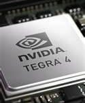
Before the opening keynotes Nvidia formally announced the Tegra 4 which is TSMC 28nm versus the Tegra 3 at 40nm. With four Cortex A15 CPU cores and 72 GPU cores the Tegra 4 is the fastest SoC on the market (my opinion). It will also be the most expensive (my opinion). Tegra 4 uses the ARM Big/Little architecture so there is a fifth ARM A7 core for power management duties. We don’t count the little cores so this is a quad core SoC.

At an opening keynote Qualcomm introduced its 2013 line of Snapdragon SoCs, the Krait 300 and Krait 400, which are faster and capable of handling UHD. The architecture improvements and Qualcomm’s use of LPDDR3 RAM have reportedly upped the performance by 40%. The Snapdragon’s quad-core’s maximum clock rate has been given a boost from 1.7 GHz to 1.9 GHz.

At the Samsung keynote the Exynos 5 Octo SoC was announced touting the first 8 processor core SoC. Again using the ARM Big/Little Architecture, Samsung attaches one ARM A7 Little to each ARM A15 Big thus the 8 processor claim, the amazing and distorting Samsung marketing machine at its finest.

I got my hands on a tablet with the Tegra 4 inside but for the life of me I can’t remember who made it. Anyway, it was the most impressive tablet I saw at the show. It was VERY fast and had the MOST impressive graphics. No info on cost or battery life though but man was it fast. It kills the iPad 3 absolutely.

The biggest difference between the current batch of SoCs is that Qualcomm and Apple do not use off the shelf ARM cores. Qualcomm and Apple both license the ARM architecture and roll their own processor cores. Qualcomm has always done this for Snapdragon but Apple A6 is the first custom processor for Apple, which is in the iPhone 5.

Why do custom cores you ask? To optimize performance, cost, and battery life of course. Apple is the best example since they control the entire device including the operating system. I have an iPhone 4s and an iPhone 5. The custom SoC in the iPhone 5 is significantly faster than the iPhone 4s and the battery lasts much longer. Samsung will follow Apple and on this as well since they also control the whole device, believe it.

I do not know for an absolute fact but I would bet more than a lunch that both the Qualcomm and Apple custom SoCs also use a Big/Little strategy. In fact, I suspect that both companies use multiple Littles to squeeze the most battery life out of the devices they inhabit so the Samsung Octo announcement really is an inside joke. News flash: We only count the big processing cores, not the little power management cores or the graphics cores otherwise we would have to come up with names with 100+ cores in them and that would be annoying.

And why did Samsung rent Bill Clinton you ask? To put a famous American face on their made in Korea brand that is why. Great fit if you ask me, Samsung and an impeached American President!

You can read more about the ARM Big/Little HERE.

Join the CES 2013 discussion HERE and qualify to win an iPad Mini!


ESD Check Methodology

ESD Check Methodology
by Paul McLellan on 01-11-2013 at 5:12 pm

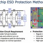
In Pune at the start of the month, Norman Chang, Ting-Sheng Ku, Jai Pollayil of Apache/Ansys and NVIDIA presented and ESD check methodologywith Fast Full-chip Static and Macro-level Dynamic Solutions . ESD stands for Elecro-Static Discharge and is basically injecting very high static voltages (think how your hand gets charged up sometimes when you touch a door handle) which can destroy a chip. This is done using three models which correspond to touching the chip with a finger (known as the Human Body Model or HBM), touching the chip with a machine such as manufacturing tester or an assembly machine known as the Machine Model or MM) and touching the chip with a tool such a tweezers or a screwdriver (known as the Charged Device Model or CDM). If the chip passes all these tests then it can survive test, assembly and shipping. And, after it has got to the consumer, the sort of abuse that people walking around on carpets or wearing silk shirts can give it. The human body model (HBM) has voltages in the KV range and the CDM has currents in the 10A range.

Here’s is one way that this is actually tested. Well, not really but there is an element of truth in it and it is very funny:

To avoid ESD destroying the chip, various protection structures are required that essentially route the charge away harmlessly so it doesn’t destroy the delicate gate-oxide in much the same way as a lightening protector does for a building (with much higher voltages). The challenge for a designer is that these structures must be verified before the chip tapes out. Finding out a chip doesn’t pass ESD tests after manufacture is a huge problem and will require a respin.


In days gone by, ESD protection was something required only in the I/O pads (so that they would defend the rest of the chip) but that no longer is sufficient and ESD cells are required in the core especially for flip-chip bumped chips where the I/Os are distributed across the die. This means that they need to be planned into the floorplan and taken acount of for their impact on other aspects of the design such as timing. Thinner oxides and reduced currents before metal interconnect acts like fuse-wire make this increasingly hard with each process generation.

There are two parts to verification of ESD. Static verification of all three models using test cases and block/IP level verification of the HBM/CD. Apache’s PathFinder is a tool that can handle all of this.


For static verification, performance and capacity are key in order to perform:

  • Fast full-chip layout-based checks

    • High-capacity and accurate metal/via resistance extraction
    • Inter- and intra-domain resistance checks
    • Realistic I-V model (snapback included) for diode/clamp in
  • R and current density checks

    • Current density and voltage check, particularly critical for IP
    • Full-chip ESD check required for identifying problems such as inter-block connectivity related
  • Macro-level dynamic ESD solution

    • Transistor-level stress analysis for 1M+ transistor blocks within couple of days
    • Consider substrate effect, clamp modeling with snapback, metal grid RLC, and pogo pin modeling

The dynamic verification must:

  • Perform diagnosis of potential failure mechanisms when silicon failures occur
  • Verify robustness of the fix by comparing differential stressed values of the failed junctions
  • Check potential design weaknesses of CDM events before tape-out on analog / mixed-signal / I/O blocks

The slides from the entire presentation, including much more detail of both PathFinder and NVIDIA’s methodology are here.


The First 14nm FinFET Wafer Sighting!

The First 14nm FinFET Wafer Sighting!
by Daniel Nenni on 01-11-2013 at 12:10 pm

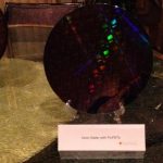
Incredibly exciting! Even my beautiful wife was impressed by the rainbow of colors it reflected. From left to right: 28nm, 20nm, and 14nm wafers. The 20nm and 14nm wafers are from the GLOBALFOUNDRIES NY fab, made in the USA! GF also announced another $3-4B CAPEX for 2013 to increase capacity of all three of their 300mm fabs (Singapore, Dresden, and NY). Strangely enough I have been to the Singapore and Dresden fabs but not NY, and my family is from upstate NY. As soon as it warms up I will visit for sure. I love hanging with the fab guys.

This was the third annual GLOBALFOUNDRIES CES party and it was definitely the best. We got there early so I got a good look at the badges laid out for everyone. I won’t out anybody but let’s just say it was the Who’s Who of the semiconductor industry and was a big tell of who their customers and close partners are. Great food too! The Mirage Hotel really knows how to do a Las Vegas style backyard BBQ.

Good thing I did not make a bet on who would have FinFETs in production first because I would have lost! Just a minor detour but I will be keynoting FinFET Day at the Electronic Design Processing (EDPS) Symposium in Monterey this April. Friday morning there will be presentations on the challenges of FinFET design by designers from the likes of Qualcomm, ARM, NVIDIA, and Oracle. In the afternoon there will be a panel on the challenges of FinFET manufacturing with TSMC, GLOBALFOUNDRIES, and hopefully Samsung and Intel. Put it on your calendar and stay tuned to SemiWiki for updates as we get closer to the event.

GLOBALFOUNDRIES at CES is a great thing. Being at the bottom as we are, it is very important to see the entire supply chain including the final products and customers. It is a great perspective which is why I come every year. That and the hotels, food, drinks, shows, gambling, I love Las Vegas.

One funny thing about the GF party, the parting gift was a very nice world travel adapter and USB charger. The sticker on the bottom however said made in China…… whoops. Any guess on how many publications “borrow” the 14nm wafer picture taken by my nifty iPhone 5?

Don’t forget to register for the Common Platform Technology Forum. It will be FinFETtastic! Just click on the banner below. Spoiler alert: Free breakfast AND lunch!

And special thanks to the Hilton for putting us in a Penthouse Suite. Living large in Las Vegas. This room is bigger than our first apartment. You should have seen the look on my wife’s face when they said 39th floor. She is afraid of heights!


Predictions are hard, especially about the future

Predictions are hard, especially about the future
by Paul McLellan on 01-11-2013 at 11:26 am

I was asked to make some predictions about the EDA, semiconductor and electronic systems markets for 2013. I decided that it would be more fun to make some plausible predictions, some of which will be right, rather than go for anodyne predictions (“Cadence will acquire a couple of startups”) which are uninformative, not to mention boring. So, drum roll, here are my 2013 predictions:

  • There will be a lot of discussion about the costs of 20nm since it is so much more than 28nm. It will be a very slow transition with some people going straight to 14/16nm (which is really 20nm with smaller transistors which is really 26nm with smaller transistors). Expect lots of discussion about the end of Moore’s law.
  • EUV lithography will not become commercial during 2013 and so will miss the 10nm node.
  • TSV-based 3D ICs will start to become mainstream. Memory on logic, and mixed digital/analog on interposer. Expect lots of discussion about “more than Moore” and how 3D is the new way for scaling.
  • The death of a giant will finally take place. Nokia, still #1 only a year ago, will be dismembered. A consortium of Apple, Google and Samsung will buy the patents for billions to stop any trolls getting any of them. Huawei will buy the handset and base-station businesses for peanuts.
  • Synopsys will acquire Mentor. EDA will otherwise be fairly boring with the big three being the only companies able to attack the upcoming problems that require dozens of tools to be updated, not just a new point tool inserted in the flow.
  • If the IPO markets are open, Jasper, eSilicon, Atrenta and Tensilica will go public. If someone doesn’t buy them first.

OK. Everyone can play this game. What are your predictions?


A Brief History of Synopsys DesignWare ® IP

A Brief History of Synopsys DesignWare ® IP
by Daniel Nenni on 01-11-2013 at 9:00 am

Let’s play word association. I say “EDA”, you immediately think “Synopsys”. I say “IP” and although 15 years ago you may not, today, you think “Synopsys”. For nearly two decades, Synopsys has grown its IP business through both organic development and acquisition, with a clear focus on enabling designers to meet their time-to-market requirements and reduce integration risk by providing the high-quality IP they need, precisely when they need it.

Today, Synopsys is considered by designers as the industry’s trusted IP partner. Its DesignWare IP is shipping in billions of chips … and counting. According to the latest research from Gartner, Synopsys is the leading provider of interface, analog and memory IP and the No. 2 provider of IP in the industry. In 2012 Synopsys achieved its 100th design win with its 28-nanometer (nm) IP and was awarded TSMC’s 2012 Interface IP Partner of the Year for the third consecutive year. These milestones, along with more than 1400 engineers and a worldwide technical support team demonstrate Synopsys’ commitment to helping customers achieve their design goals at every step. The world of IP is definitely changing. With the shift to IP subsystems, 20-nm IP and FinFET, Synopsys remains in the forefront of providing the IP needed for these technology advancements. Figure 1: Synopsys’ Growing IP Business:

So How Did Synopsys Get Here?
In the 1990s Synopsys launched the DesignWare Foundation Library, a collection of technology-independent, reusable building block IP such as adders and multipliers that are tightly integrated with Synopsys’ synthesis environment, delivering significant improvements in area, timing and runtime. Through the years, complex IP blocks were added to the library such as 8-bit microcontrollers, AMBA on-chip bus IP as well as verification IP (a.k.a. SmartModels). With these additions, the product became known as the DesignWare Library – and it has been the most widely used library of foundation IP ever since.

Fast forward a decade. We saw an explosion in the usage of standards-based communication protocols, setting the stage for the emergence of the commercial IP industry as companies realized they needed to focus their efforts on the differentiated portions of their design and not on developing standards-based IP. In 2002, Synopsys acquired inSilicon, adding popular interface protocols such as PCI-X, USB, IEEE 1394 and JPEG to its DesignWare IP portfolio. By 2004, Synopsys was seeing increased demand in PCI Express (PCIe) for data center and server applications. By acquiring Cascade Semiconductor, Synopsys rounded out its already successful DesignWare PCI Express Endpoint solution with root port, dual mode and switch ports, providing designers with a complete high-performance, low-latency PCI Express IP solution. Also in 2004, the acquisition of Accelerant Networks brought serializer-deserializer (SerDes) technology to Synopsys. Figure 2: DesignWare PCI Express IP Solution:

In 2007, Synopsys released the DesignWare USB 2.0 nanoPHY, its next-generation USB 2.0 PHY, which cut the power and size in half over the previous generation. The expansion of Synopsys’ IP portfolio continued that year with the launch of digital controllers for PCI Express 2.0 (5.0 GT/s), mobile storage, SATA AHCI and the acquisition of Mosaid’s DDR memory controllers and PHY IP. One year later, Synopsys continued its momentum in DDR by releasing a full range of silicon-proven DDR3 and DDR2 IP solutions and announced a complete SuperSpeed USB 3.0 IP solution.

In 2009, Synopsys moved into the analog IP business with the acquisition of the Analog Business Group of MIPS Technologies. The acquisition added to the DesignWare IP portfolio a new family of analog IP such as analog-to-digital converters (ADCs), digital-to-analog converters (DACs) and audio codecs. It also added HDMI 1.3 transmitter (Tx) and receiver (Rx) IP to Synopsys’ existing interface portfolio. With this acquisition, designers were able to go to a single, trusted vendor for both their analog and interface IP needs. In the same year, Synopsys introduced new products such as minPower Components; Ethernet IP with support for the IEEE 1588 specification; DDR3 IP operating at 2133 Mbps data rate and 1.35V DDR3L, SATA 6 Gbps digital controllers; and a complete solution for PCI Express 3.0 (8.0 GT/s).

The acquisition of Virage Logic in 2009 added logic libraries and embedded memories, enabling designers to achieve the best combination of power, performance and yield; memory test and repair; non-volatile memory; and ARC processors targeted at embedded and deeply embedded applications. Throughout 2010, Synopsys continued to introduce new products that would help designers integrate advanced functionality into their SoCs such as:

  • Third -generation USB 2.0 PHY – the USB 2.0 picoPHY (30% smaller area and lower power compared to the previous generation)
  • 40-nm data converters
  • Universal DDR controllers supporting DDR2, DDR3, Mobile DDR and LPDDR2 standards
  • DDR multiPHY supporting six DDR standards
  • MIPI 3G DigRF, DigRF v4, CSI-2 controller, DSI host controller and D-PHY
  • HDMI 1.4 Tx/Rx controller and PHY
  • Ethernet controller with an audio-video bridging feature
  • DesignWare STAR ECC (error-correcting codes)
  • ARC processor cores for Blu-ray Disc players

In 2011, the focus was on helping designers develop 28-nm SoCs. Synopsys announced the availability of DesignWare Interface PHY and Embedded Memory IP for TSMC’s advanced 28-nm process as well as the collaboration with UMC on embedded memory and logic library in 28-nm. Significant milestones were also achieved, including Synopsys’ DesignWare STAR Memory System being shipped in one billion chips, DesignWare SuperSpeed USB 3.0 IP achieving more than 40 design wins, and GUC taping out 30 customer chips using DesignWare IP. The DesignWare ARC EM processor family for embedded applications was also launched this year.

In 2012, designers started to integrate more and larger third-party IP into SoCs, it wasn’t enough to just provide individual IP blocks – the market needed complete IP subsystems to ease the integration effort. In March 2012, Synopsys unveiled the industry’s first complete, pre-integrated and configurable audio subsystem consisting of hardware, software and prototyping. Figure 3: DesignWare SoundWave Audio Subsystem:

In the same year, Synopsys also had significant IP product releases such as the industry’s first 28-nm Multi-Gear MIPI M-PHY IP supporting six standards, DDR4 memory controller and PHY, MIPI UniPro and UFS, STAR Memory System for 20-nm designs and IP for the SMIC 40-nm low leakage process.

With more functionality going into a single device, third-party IP continues help designers reduce risk and speed time-to-market. Based on Synopsys user surveys, the top five criteria for selecting an IP provider are:

[LIST=1]

  • IP technology leadership
  • Quality/silicon-proven IP
  • Market leadership
  • Brand reputation, and
  • Breadth of IP portfolioThese have been Synopsys’ IP priorities as well.To learn about all the DesignWare IP developments, visit the website.


TSMC Apple Rumors Debunked!

TSMC Apple Rumors Debunked!
by Daniel Nenni on 01-11-2013 at 8:00 am

Disclaimer: I’m a blogger and by definition I share my observations, opinions, and experiences. Journalists and Analysts on the other hand are held to a much higher legal standard which is why they cite undisclosed sources and use double speak to shield themselves legally. Why trust a SemiWiki blogger over a Journalist or an Analyst? Because we actually work inside the fabless semiconductor ecosystem and they do not, simple as that. My previous TSMC blogs are HERE if you want to check my credentials. Be sure and read the ones early last year on the rumors of problems with TSMC 28nm. I said FALSE and I was right, the Journalists and Analysts were wrong, and their pants are on fire once again.

The first rumor is that the next Apple A7 processor (28nm) will be made by TSMC. That rumor is FALSE! As I previously blogged, the Apple iPhone to be released this year (iPhone 5s) will be Samsung 28nm. The iPhone to be released next year (iPhone 6) will be TSMC 20nm. A company the size of Apple cannot switch foundries on a moment’s notice. The volumes are too high and the technology issues are too complex.I have no doubt Apple discussed 28nm with TSMC but since no other foundries had 28nm available there was no way TSMC could handle the wafer demands of Apple and the rest of the fabless companies. Apple also gets preferred pricing so why would TSMC give up higher margin 28nm business AND alienate their customer base? Not going to happen.

TSMC: Our mission is to be the trustedtechnology and capacity provider of the global logic IC industry for years to come.

20nm will be another story. Samsung and GLOBALFOUDNRIES will have 20nm in production and TSMC will see their 28nm customers use other sources. Qualcomm, TI, Broadcom, Marvell, and Xilinx all second and third source wafer manufacturing when possible. 20nm volumes will also not match 28nm due to a higher cost per transistor. To me 20nm is a half node in the economic sense in preparation for 16/14nm FinFETs, which will hit much higher volumes from the mobile guys due to lower power consumption (longer battery life).

The second rumor is that TSMC will build a fab in New York to help facilitate Apple business. I say FALSE. If TSMC builds a GigaFab anywhere in the United States I will eat my SemiWiki hat, simple as that.If TSMC needs to expand capacity above and beyond what they have planned today they can simply take over empty DRAM fab space in Taiwan which there is plenty of. Or if you want a more realistic rumor to spread here it is: TSMC will acquire the #3 semiconductor foundry UMC to increase capacity. This is much better than the rumor last year that GLOBALFOUNDRIES would acquire UMC. But I don’t do rumors so you didn’t hear it from me.

The Taiwan government founded the pure-play semiconductor foundry business working hand-in-hand with both TSMC and UMC. TSMC and UMC are brothers. The Taiwan economy is semiconductor centric. TSMC is one of Taiwan’s top employers. I have no doubt that TSMC is seriously looking at all options but why would they follow the GLOBALFOUNDRIES model of having “global foundries” in favor of the TSMC model of Taiwan based cost efficiencies? The U.S. environmental impact bureaucracy alone would kill that deal! :p The wafer business has always been about price and that will never change.The other prediction I made last year is that TSMC stock (TSM) is a $20 dollar stock. It will happen this year, believe it.That’s my story and I’m sticking to it.

Related: Apple will NOT manufacture SoCs at Intel!


Reducing Dynamic and Static Power in Memories

Reducing Dynamic and Static Power in Memories
by Paul McLellan on 01-10-2013 at 3:46 pm

Sequential approaches to power reduction work well on logic implemented using standard cells. But part of every SoC, sometimes a very large part, is taken up with embedded memories for which alternative approaches are required. Not only do these memories occupy up to half of the area they also account for as much as 75% of the power dissipation, a mixture of static (leakage) and dynamic power.

The basic idea of how to reduce dynamic power in memories is simple: if you are going to read the same address as last time then don’t bother to do the read, just use the old latched value. Similarly, if you are going to write the same value as last time to the same location, then don’t bother with the write since it has no effect. Of course, both these will save the most power when the address remains stable for large numbers of clock cycles.

Designers know this, of course, and over time they try and analyze the registers for redundant accesses and look for opportunities to shut them off. Doing this automatically during synthesis is beyond the scope of RTL synthesis tools. But doing it manually can be error-prone. Missed opportunities to shut-off redundant access results in less than the maximum power saving. Worse, shutting off an access that turns out not to be redundant will result in an error (reading the wrong value, for example) and probably a very obscure system failure.

Sequential analysis involves analyzing the entire design, including memories. It looks over a window of several clock cycles to find which values are propagated, which changes are not observable, which registers are known to remain unchanged. This is the basis for power optimization which results in shutting off unused or unobservable computations, preventing “new” values from propagating when they are known to be the same as the old value and so forth.

The same approach can be used with embedded memories. Even though at first glance every read and write to memory may seem to be essential, depending on the control sequence of the design they may not be required. Removing such redundant accesses typically results in significant reduction in the dynamic power consumption of memories.


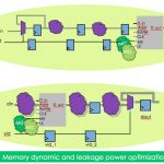
For a specific example, with the Synopsys/Virage 40nm memory above, the memory enable can potentially be held low for long periods, saving dynamic power.

Embedded memory vendors provide capabilities to reduce not just dynamic power but also static leakage power in memories that are not in use. These involve sleep and wake signals but, in turn, that means logic to create those signals. Of course this is a tradeoff: the power saving from the sleep mode has to be greater than the power taken up generating those signals, but as long as memories are sometimes put to sleep for many clock cycles, this balance is likely to be positive.


Again, using the same Synopsys/Virage memory, further savings are possible by generating appropriate sleep signals, taking into account the requirement that the memory takes an extra clock cycle to wake.

These two optimizations work together powerfully. The more redundant accesses are suppressed, the more the memory is idle and so can be put into a sleep mode saving even more dynamic and leakage power.

Calypto’s PowerPro is a sequential power optimization tool capable of doing deep sequential analysis of the whole design, including memories, and either guides designers to make manual changes safely, or automatically updates the RTL to produced a power-optimized version.

There will be a webinar on reducing dynamic and leakage power in memories on Tuesday February 12th at 10am Pacific time. Webinar details, including registration, are here. There is a white-paper on the same topic on the Calypto download page here(look for Memory Power Reduction in SoC Designs Using PowerPro MG).