

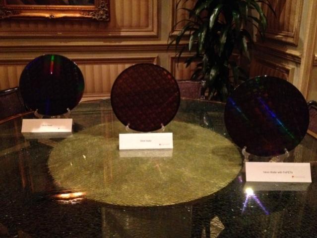
 Incredibly exciting! Even my beautiful wife was impressed by the rainbow of colors it reflected. From left to right: 28nm, 20nm, and 14nm wafers. The 20nm and 14nm wafers are from the GLOBALFOUNDRIES NY fab, made in the USA! GF also announced another $3-4B CAPEX for 2013 to increase capacity of all three of their 300mm fabs (Singapore, Dresden, and NY). Strangely enough I have been to the Singapore and Dresden fabs but not NY, and my family is from upstate NY. As soon as it warms up I will visit for sure. I love hanging with the fab guys.
This was the third annual GLOBALFOUNDRIES CES party and it was definitely the best. We got there early so I got a good look at the badges laid out for everyone. I won’t out anybody but let’s just say it was the Who’s Who of the semiconductor industry and was a big tell of who their customers and close partners are. Great food too! The Mirage Hotel really knows how to do a Las Vegas style backyard BBQ.
 Good thing I did not make a bet on who would have FinFETs in production first because I would have lost! Just a minor detour but I will be keynoting FinFET Day at the Electronic Design Processing (EDPS) Symposium in Monterey this April. Friday morning there will be presentations on the challenges of FinFET design by designers from the likes of Qualcomm, ARM, NVIDIA, and Oracle. In the afternoon there will be a panel on the challenges of FinFET manufacturing with TSMC, GLOBALFOUNDRIES, and hopefully Samsung and Intel. Put it on your calendar and stay tuned to SemiWiki for updates as we get closer to the event.
GLOBALFOUNDRIES at CES is a great thing. Being at the bottom as we are, it is very important to see the entire supply chain including the final products and customers. It is a great perspective which is why I come every year. That and the hotels, food, drinks, shows, gambling, I love Las Vegas.
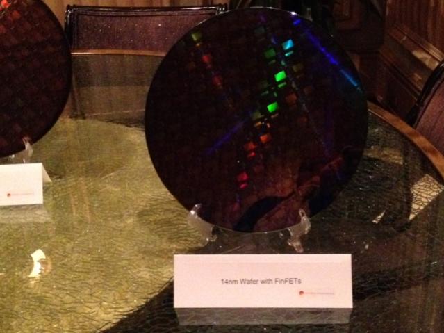
One funny thing about the GF party, the parting gift was a very nice world travel adapter and USB charger. The sticker on the bottom however said made in China…… whoops.  Any guess on how many publications “borrow” the 14nm wafer picture taken by my nifty iPhone 5?
Don’t forget to register for the Common Platform Technology Forum. It will be FinFETtastic! Just click on the banner below. Spoiler alert: Free breakfast AND lunch!
And special thanks to the Hilton for putting us in a Penthouse Suite. Living large in Las Vegas. This room is bigger than our first apartment. You should have seen the look on my wife’s face when they said 39th floor. She is afraid of heights!


TSMC CoWoS versus Intel EMIB Semiconductor Packaging