Bronco Webinar 800x100 1

Global Design Closure

Global Design Closure
by Paul McLellan on 01-09-2013 at 8:34 pm

Satish Soman, chief solutions architect at Atrenta, was invited to give a presentation on Global Design Closure at the VLSI India conference in Pune at the start of this month. He talked about the need to close the gap between the typical SoC development methodology and what happens in reality.


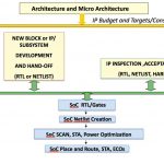
SoCs are really put together in two phases. Block level or IP design is done and the RTL designers do what they can to verify not just functionality but whether the block will meet its performance specifications when put into the SoC. These blocks are handed off at the RTL level to the SoC design team who create the final netlist, do place and route, timing analysis, test insertion and so on.

The reality of what is actually handed off is that it is verified RTL, with verified constraints and verified testability (which are all straightforward to do at the RTL level). What is not handed off is any block-level physical awareness, any context of how the block will be used in the SoC, and there is no feed-forward of physical information about the block or IP.

This shows up as long and unpredictable SoC design closure cycles, with difficult iteration back to the RTL design teams (which are often geographically remote from the SoC design team). Current attempts to alleviate the pain are to do early drops to the physical design team, provide the RTL team with physical tools and so on. Basically get early feedback of the missing information.

SpyGlass Physical is Atrenta’s tool for addressing this. It is a tool for the RTL designer that gives them a dashboard for analyzing and addressing congestion and other physical issues at the block/IP design start, prior to RTL handoff to the SoC assembly team. It is also used a the SoC level to get similar information (plus, of course, additional features for padring, I/O etc) without having to go through a complete iteration of synthesis and physical design which typically takes several days.


Using SpyGlass Physical during RTL design will slightly increase the time taken before RTL is ready for handoff. But the RTL will be of superior quality and so the synthesis and place & route will be much reduced, as will iterations back to fix RTL issues that manifest themselves as physical design issues such as routing congestion.

Oasys RealTime Explorer

Oasys RealTime Explorer
by Paul McLellan on 01-09-2013 at 8:00 am

The current methodology in design in most companies, and certainly many of the biggest, is that front end RTL design is done by one team with a limited set of front-end design tools. This is then eventually passed off to the physical design team who run all the scripts, do the “real” synthesis, place & route and timing verification. Essentially we have two separate groups with RTL handoff between them. This methodology worked fine for 1M gate designs a couple of process nodes ago. It doesn’t work for 10M and 100M gate designs.

In practice what happens is that everything looks fine to the front-end designers who are looking at individual blocks without the true physical information. They may be using approximate synthesis and are certainly using approximate physical information. When the back end team put the whole design together there are dozens if not hundreds of violations that need to be resolved by passing the design back to the front end designers to change the RTL. Simply redoing the design using different constraints or different scripts is not good enough.

Add to this the increasing tendency to use an offshore group of comparatively inexperienced designers to do all the front end design and this is a recipe for trouble. It takes about 3 days or so to run a design all the way through the back end, although sometimes the engineers just are not available (especially during a critical tapeout) and it can take weeks to get anything beyond the most basic feedback.


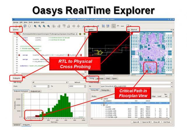
RTL engineers, not just the back end team who run the real synthesis of the entire design, need to be able to visualize and interact with the physical RTL results of their synthesis. But, critically, not at the block level but the entire design. Since RTL level blocks will be grouped into the physical hierarchy, block level information is fundamentally incorrect. This enables them to produce higher quality RTL that is free of top-level timing violations, routing congestion, designs that are too big for the floorplan or the power budget.

Of course the two things to make this possible are capacity (so that the entire design can be synthesized and analyzed as a whole) and speed (since RTL designers aren’t going to sit around for days waiting to find out what they need). Oasys’s RealTime technology, already used in RealTime Designer, is now available in RealTime Explorer, which is targeted specifically at making the front-end designer more effective and eliminating iterations between the frontend and backend design teams.


A simple-to-explain example is when a very wide multiplexor causes routing congestion. This cannot be fixed effectively in the back end. Someone who understands what the multiplexor is really doing needs to alter the RTL to something better. Just tightening the timing constraints isn’t going to do it.

Bottom line: RTL engineers can eliminate their dependence on physical design teams for top level timing & routability analysis.

More information on Oasys’s (new) website here.

UPDATE: there is a webinar on RealTime Explorer every couple of days from January 15th to 31st. Details on the webinar page here.


Interface Protocols, USB3, PCI Express, MIPI, SATA… the winners and losers in 2012

Interface Protocols, USB3, PCI Express, MIPI, SATA… the winners and losers in 2012
by Eric Esteve on 01-08-2013 at 5:25 am

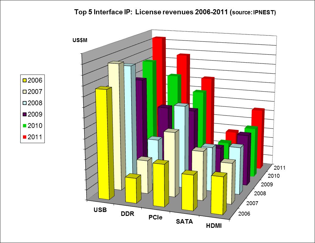
Who makes the decision and declare that a specific interface protocol is successful? Not me, as I can only consolidate market share data and some insight information coming from the industry. The end user, when going to a shop (real or virtual) and spend a significant part of his budget to buy an electronic product, selecting among hundreds, will eventually decide for the success of a certain feature (SuperSpeed USB, HDMI or ThunderBolt). But, if you wait for the success of this feature on the mainstream market to integrate it into your system (OEM), your SoC (chip maker) or your IP portfolio (EDA/IP vendor), then you are respectively 12/18 months, 2 years or more late…
Continue reading “Interface Protocols, USB3, PCI Express, MIPI, SATA… the winners and losers in 2012”


OTP @ 2013 Common Platform Technology Forum

OTP @ 2013 Common Platform Technology Forum
by Daniel Nenni on 01-06-2013 at 9:00 pm

Sidense will be exhibiting at the Common Platform Technology Forum in Santa Clara, California on February 5, during which time they will be discussing their one-transistor, one-time programmable (1T-OTP) memory IP products. Based on their patented 1T-Fuse™ bit cell, Sidense antifuse-based 1T-OTP macros offer a secure, reliable, low-cost and field-programmable alternative solution to mask ROM, eFuse, EEPROM and flash memory technologies in many applications.

Sidense Corp. provides secure, very dense and reliable non-volatile, one-time programmable (OTP) memory IP for use in standard-logic CMOS processes with no additional masks or process steps required. The Company’s innovative one-transistor 1T-Fuse™ architecture provides the industry’s smallest footprint, most reliable and lowest power Logic Non-Volatile Memory (LNVM) IP solution. With over 100 patents granted or pending, Sidense OTP provides a field-programmable alternative solution to Flash, mask ROM and eFuse in many OTP and MTP applications.

Sidense 1T-OTP macros are implemented in standard logic CMOS processes and need no additional masks or process steps. The macros are available at many process nodes and variants, including BCD and high-voltage nodes, from 180nm down to 28nm from leading top-tier foundries and selected IDMs. Sidense macros are available in densities up to 512 Kbits per macro, which can be combined to implement several megabits of storage on a chip. Sidense offers some products with read and programming capability up to 150ºC, ideal for automotive “under the hood” applications. Programming may be done at test, at wafer probe, or in the field from an external source or with an on-chip charge pump.

1T-OTP macros are inherently low power, making them ideal storage choices for mobile communications and other handheld devices. Designers are using Sidense 1T-OTP for code and key storage, look-up table data, processor and logic configuration, ID tags, and analog trimming and calibration. Typical applications include sensor conditioning, power management, display drivers, image processors, network controllers, wireless LAN and Bluetooth controllers for the automotive, mobile, commercial and industrial market segments.

Sidense 1T-OTP is now licensed to more than 100 customers including several of the top semiconductor manufacturers and is now designed into devices in mass production in all major semiconductor markets including: media processors, display drivers, automotive sensors, image sensors, wireless peripherals and microcontrollers. 1T-OTP is available with more than 10 foundry partners and IDMs including all top-tier foundries. Sidense also broadened the process node availability from 180nm to 28nm for the Company’s products. To further align the portfolio with customers’ requirements, 1T-OTP has been ported to power/BCD processes qualified for automotive applications and high-voltage processes for display drivers.

For more information, please go to www.sidense.com and visit Sidense at the Common Platform Technology Forum in Santa Clara, California on February 5, 2013:

General Agenda:

  • 8:30am – 9:00am Registration and Continental Breakfast
  • 9:00am – 11:30am Keynote Session
  • 11:30am – 1:00pm Lunch / Exhibit Area Open
  • 1:00pm – 4:40pm Technical Session
  • 4:40pm – 6:00pm Reception

Partner Exhibit Hours:

  • 11:30am – 6:00pm

Who said there is no such thing as a free lunch! I hope to see you there!


Will Google Go Thermonuclear?

Will Google Go Thermonuclear?
by Ed McKernan on 01-06-2013 at 8:30 pm

“It’s not like we started it,” said Larry. “After all the idea of going Thermonuclear was first broached by Steve to Eric at their outdoor café meeting in Palo Alto way back in 2010. We’re just following by example and as Steve was wont to quote Picasso; “good artist copy, great artist steal” so why not go Thermonuclear with our Android partners before they get too large and unmanageable. The stakes are too high not to take things into our own hands and the X-Phone will be the start – however we’ll need some new partners to help carry the load. Let’s just remember that whatever we do, make sure there’s no evil involved.”

The shifting Mobile Tectonic plates are bound to create new partnerships and alliances as the old Wintel empire retreats to its legacy comfort zone. What remains today are four players looking to dominate the mobile platform (i.e. Apple, Google, Samsung and Amazon) and each need to expand their presence in the coming new year or fall behind. Recent rumors abound that Amazon is going to build a smartphone; Google will create its X-Phone to outflank Samsung who in response is hedging its O/S options with Tizen, another mobile Linux O/S that is also backed by Intel. Get the picture: trust no one, especially not your “partners.”

Apple’s introduction of the iPAD Mini is one more step in the race to solidify the standardization of form factors based on whether it is a one-handed or two-handed mobile device. It is now clear that true personal mobility will be encased in a device that holds a screen that is between 4 and 8” and costs from $0 subsidized to $699 unsubsidized with the latest baseband technologies at the high end. In this expanded market place one can include iPods, smartphones, tablets and e-readers. This eventually becomes a market of multiple billions of units a year and served only by those who can assemble a very efficient integrated supply chain like Apple and Samsung do today. Over the past year, Google has come to understand that these former partners will be strict gatekeepers who intend to exclude their maps icon from the devices that fall into a new customers hand. Savvy buyers will know hoe to upgrade but many will stay with the default settings and thus deny Google revenue. Amazon also knows that their marketplace will depend on mobile shoppers who don’t have a one button access to their web site. The current Kindle platform is not feature rich enough to attract premium buyers.

Legacy is still profitable for Wintel but is likely to shrink in terms of dollars in a manner similar to how IBM’s mainframe business declined. The original 10” iPAD, we can now say was Apple’s way to test the market on the concept of internet consumption being more important than the Microsoft Office Suite. Consumers were expected to dabble but would corporate? The answer in the end was yes and it caught Intel and Microsoft by surprise because it was underpowered and didn’t support traditional apps. Intel received their heads up from Transmeta in 2000 on the importance of battery life in a wireless world but spent the next ten years pushing performance in large notebooks.

While Apple shipped iPADs with $30 processors, Intel launched Sandy Bridge and Ivy Bridge “ultra low voltage” parts at premium prices (>$200) and thus not only stunted the launch of ultrabooks but also tablets. Apple’s model can be summarized as giving away the processor, graphics and iOS while getting paid a premium on Batter Life, NAND storage and 4G LTE. In the end, the high valued piece of computing that Moore’s Law addresses is that which is most mobile and connected. Intel could have vectored off the performance roadmap years ago to build an ultra low power x86 that was economical, but perhaps they were too distracted by AMD and NVidia. I have a strong suspicion that Apple understood that Wintel would breakup based on each vendors desire to maintain their high margin component and compromise was out of the question. Microsoft’s decision to build their own tablet with an ARM processor shows that it is late in the game. And so Apple’s model to give away the processor and O/S is in many ways similar to Microsoft giving away Internet Explorer for Free in order to dispatch the once thriving upstart known as Netscape. One can hear the oxygen being sucked out of the room.

In the coming year Apple and Samsung will look to extend their leads as they ping pong faster product iterations to close the gaps that once existed between a 3.5” iphone and a 10” tablet. Look for an iPAD mini refresh with a Retina Display in the months ahead that will be priced at $359 and allow the current device to drop to $299. Also look for an iPod with a 5” display as well as a new iPhone with a larger display, better camera and NFC. Samsung will splatter the wall with even more versions at ever smaller price point increments as they leave no product hole. Google sees this coming and has to move quickly or lose its leverage.

The issue for Google is not just the creation of the X-Phone, it also entails the creation of a whole supply chain and retail stores or stores within stores. Android started as an O/S that was meant to be proliferated to multiple OEMs who each took a small slice of the pie and thereby enable the creation of the equivalent Microsoft’s PC strategy for the current decade. Samsung took the free O/S and leveraged its incredible vertical supply chain and fantastically expensive marketing budgets to buy off the channel while still making a profit. The other Android players withered at the assault. And so now Google has to conjure up advanced products to outflank Samsung. Google will need help on the hardware side. Will they turn to Intel as a Fab for cheap mobile chips and in return swear to stay x86 in their data centers. Is Amazon thinking the same thing?

Apple’s plan to ramp at TSMC this year with its A6X processor is a sign that they are looking to be completely independent of Samsung in the next 18 months. If they were unable to make a deal with Intel as a second Foundry then the latter has to aggressively move to partner with one of the other platform players. Paul Otellini sits on Google’s Board and I am sure has made the pitch. Is there a conflict of interest here that has caused him to resign from Intel early in order to facilitate a partnership? Time will tell. However mistakes at this stage will be magnified down the line. Where we sit today was unimaginable a year ago and where we sit January 2014 is likely to be significantly beyond what we can now dream.


Full Disclosure: I am Long AAPL, INTC, ALTR, QCOM


Celebrity Electronics Show 2013 (CES)

Celebrity Electronics Show 2013 (CES)
by Daniel Nenni on 01-06-2013 at 4:00 pm

Time to pack up for the 2013 Consumer Electronics Show in Las Vegas, I will be driving down with my beautiful wife Shushana because she does not like to fly. The drive takes the better part of a day so we will leave early and see the sunrise over the desert. She is great company, the time will fly by. We will be 2 of the more than 150,000 people to attend this year. Wow!

Last year’s celebrities included: Basketball bad boy Dennis Rodman, Fitness guru Jillian Michaels, Gadget fan boy Justin Bieber, Rapper 50 Cent, Reality stars PaulyD and Snooki, Actor Will Smith, Singer Kelly Clarkson, Ryan Seacrest, Rapper/Actor LL Cool J, and Justin Timberlake, just to name the most famous ones. No telling what CES has in store for us this year. Rumor has it Bill Clinton will be here (surrounded by booth babes I will bet) which would be worth the wait.

Since I’m on the CES press list I have been pelted with emails on what to expect this year. Last year the OLED HD TV’s were the coolest. Unfortunately I need a 63” to replace my current plasma screen and OLEDs only come in 55” so I will wait. Same thing with Apple TVs I’m told, 55” is the sweet spot. Ultrabooks were big last year but I have yet to buy one. I recently bought (2) HP laptops since they were half the cost of Ultrabooks. We are a smartphone/tablet family now so laptops are only for work that is easier on a laptop like blogging and QuickBooks. Samsung had the biggest booth last year with the most impressive collection of phones and tablets. It will be interesting to see who challenges Samsung this time (Apple doesn’t go to CES).

This year it’s TV Tablets, Google TVs, and a new Smart TV from Samsung that all other TVs are rushing to see:

One of the most interesting new products will be flexible screens from Samsung which will be 5.5″ bendy displays with a resolution of 1280 x 720 HD and a pixel count of 267 ppi. Nothing like getting twisted in Las Vegas!

A Red Ridge Tablet from Intel? Red Ridge is Intel’s Medfield-based tablet platform, which is definitely blog worthy and from what I have read it is already in production. More on that after I get to see/touch one.

Intel will also talk in detail about actual 22nm mobile SoCs. The Bay Trail-T is rumored to be a quad-core scheduled for a 2014 launch and the Valleyview-T which will take on NVIDIA’s Tegra 3 and Qualcomm’s S4.

In a counter announcement, NVIDIA will show the Tegra 4 which is TSMC 28nm (my all time favorite process node). Tegra 3 is TSMC 40nm and has done quite well in the HTC One X+ and tablets such as Google’s Nexus 7 and Microsoft’s Surface. Tegra 4 is a quad core ARM A15 SoC with monster graphic capabilities. I would bet there will be Tegra 4 based tablets at the show.

Cars were pretty big last year but this week even more so. Audi, Chrysler, Ford, General Motors, Hyundai, Kia, Subaru and more than 100 auto tech companies displaying the latest in-car technology. Lots of fitness and health related products too making bio engineering and robot people even closer to reality.

OK, that’s my 600 words for today. It would be a pleasure to meet you if you are in Las Vegas this week. I will definitely be at the GOLBALFOUNDRIES party on Wednesday night. This is their third year at CES and I congratulate them for bringing the fabless semiconductor ecosystem to Las Vegas. After all, this is where our customers are.

Joinn the CES 2013 discussion HERE.


Online Schematic Capture and SPICE Circuit Simulation

Online Schematic Capture and SPICE Circuit Simulation
by Daniel Payne on 01-04-2013 at 11:33 pm

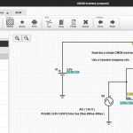
I love all things SPICE so when I read a tweet tonight from @PartSimI just had to try out their Schematic Capture and SPICE circuit simulator in a browser. The site is www.partsim.com and all you need is a web browser and short registration process, then it’s off to the Examples where I found a simple CMOS inverter and then extended it to be two inverters:


Continue reading “Online Schematic Capture and SPICE Circuit Simulation”


Tech Forum, February 5, features 32/28-, 20-, 14-, and 10-nanometer processes

Tech Forum, February 5, features 32/28-, 20-, 14-, and 10-nanometer processes
by Daniel Nenni on 01-04-2013 at 7:00 pm

The Common Platform Alliance — IBM, Samsung Electronics, Co., Ltd., and GLOBALFOUNDRIES — continues to redefine the landscape of the semiconductor industry with its groundbreaking collaboration. Join us at our 2013 Common Platform Technology Forumon Tuesday, February 5, 2013 at the Santa Clara Convention Center as we showcase the latest technological advances being delivered to the world’s leading electronics companies.


Real Collaboration = Big Business


At the Common Platform Technology Forum, you’ll see and hear firsthand how the combined expertise of our partners is addressing the most demanding IC design and manufacturing challenges. Our collaborative research and innovative technology development have resulted in an accelerated roadmap and rapid customer adoption, and we’ll touch upon these key highlights:

    [*=left]Leading-edge process technologies at 32/28-, 20-, 14-, and 10 nanometer
    [*=left]Advanced innovations such as FinFET, design & technology co-optimization, and double patterning

Plus:

    [*=left]A peek into the future of next-generation device innovations being researched: silicon nanowires, carbon nanotubes, and 3D device structures
    [*=left]A showcase of our ecosystem partners and Common Platform design, enablement, and implementation offerings in our Partner Pavilion

And, visionary keynotes by IBM, Samsung, GLOBALFOUNDRIES, and ARM.

Register now for this FREE technical event!


Audio/Voice DSP IP core: the next road to billion unit shipment

Audio/Voice DSP IP core: the next road to billion unit shipment
by Eric Esteve on 01-04-2013 at 6:09 am

When mentioning CEVA DSP IP cores, the first reaction is to think about the complexes DSP functions used into wireless Modem Application like 3G and Long Term Evolution (LTE). Considering that CEVA market share is above 70% for these products, such a reaction makes sense. But did you knew that CEVA DSP IP cores are also empowering audio/voice devices, in wireless (handset, smartphones) applications requiring ultra low power consumption, as well as in consumer oriented (non wireless) applications, where the highest performance is key?

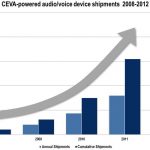
If you still have a doubt about CEVA positioning in this field, just have a look at CEVA–powered audio/voice device (ie: IC, not cores!) shipments over 2008-2012: more than 2 Billion cumulated shipments of IC integrating CEVA DSP IP cores tailored for audio or voice application:

The explosion of smartphones shipments has obviously put a strong focus on the Application processor and Baseband modem shipments, respectively empowered by the main CPU and DSP IP cores, delivered by ARM Ltd. and CEVA respectively. But, as well as ARM is investing the graphic market with their MALI GPU core family, CEVA has invested the Audio/Voice market with the Teak Lite family. Looking at smartphone block diagram, you can find this DSP located in three main places:

[LIST=1]

  • Audio/Voice processing in dedicated DSP within Baseband Processor

    • Super wideband voice codecs, noise reduction, echo canceller, audio codecs

    [LIST=1]

  • Audio offloading to dedicated audio DSP in Application Processor

    • Low power audio codecs (long playback time), post processing (e.g. DM3+)

    [LIST=1]

  • DSP integrated within or in conjunction with audio/voice CODEC chip

    • Ultra-low power voice processing (e.g. voice trigger), noise reduction, audio PP

    As usual, a precise picture (Credit: The Linley Group) will help to clearly understand the DSP positioning within (1), (2) and (3):

    It’s impressive to see how voice processing in mobile handsets is allocated with increasing DSP MIPS (200-300MHz today), to meet new requirements (higher bandwidth vocoders, noise suppression, ANC like in the iPhone 5 and more), calling for Audio/Voice dedicated DSP offering up to 500 MHz MIPS in the very near future, say in 2015.

    The race for performance is even more critical in CE market segments, with emergence of connected or smart TV, integrating camera and microphones. CEVA proposes a solid roadmap for the Teak Lite (TL) 32 bit DSP core family:

    the TeakLite III is being integrated in products shipping today in production, allowing customers to implement their own software in the audio codec to help differentiate their products from the competition.

    The next architecture generation based on the TeakLite 4 DSP core, will offer a framework of Application Specific DSP IP core, in order to provide the best Power/Performance/Area (PPA) optimization for the targeted application, including the future high end home or gaming applications, yet to come, that will require even higher performances for audio/voice processing – the 500 MHz MIPS already mentioned.

    The TeakLite 4 DSP IP core family is more than just another DSP IP core, CEVA understood how efficient it was for customers to benefit from a platform, rather than simply a naked core. That is, the platform offer integrates the various folowing features, I should say differentiators:

    • Most powerful audio/voice DSP

      • Dual 32-bit MAC, quad 16-bit MAC
      • 1.5 GHz at 28nm HPM
      • Variable 10 stage pipeline
    • Special emphasis on power optimization
    • Extensive audio/voice SW library (with more than 100 SW codecs and functions by CEVA and partners)
    • Area optimized, down to 90K gates (Small memory footprint, using 16 and 32-bit instruction width)
    • Extensible architecture, allowing customer differentiation and user defined ISA

    Last, but not least, CEVA has understood very early that the success of a processor core (whether it’s a CPU, DSP or GPU) will not only be based on the most advanced architecture (necessary condition, but not sufficing) but also on the long term building of a large ecosystem, made of SW developers partners, IP vendors, Silicon Foundries, EDA tools vendors… and satisfied customers! Sounds familiar when you remind how ARM Ltd has built his position of #1 IP vendor. Both companies are on the same track, one with CPU, the other with DSP, and we don’t see how they could lose their respective leader position, one with DSP (CEVA), one with CPU (ARM).

    Eric Esteve from IPNEST