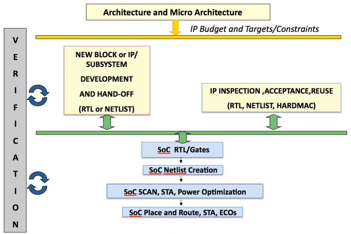


Satish Soman, chief solutions architect at Atrenta, was invited to give a presentation on Global Design Closure at the VLSI India conference in Pune at the start of this month. He talked about the need to close the gap between the typical SoC development methodology and what happens in reality.

SoCs are really put together in two phases. Block level or IP design is done and the RTL designers do what they can to verify not just functionality but whether the block will meet its performance specifications when put into the SoC. These blocks are handed off at the RTL level to the SoC design team who create the final netlist, do place and route, timing analysis, test insertion and so on.
The reality of what is actually handed off is that it is verified RTL, with verified constraints and verified testability (which are all straightforward to do at the RTL level). What is not handed off is any block-level physical awareness, any context of how the block will be used in the SoC, and there is no feed-forward of physical information about the block or IP.
This shows up as long and unpredictable SoC design closure cycles, with difficult iteration back to the RTL design teams (which are often geographically remote from the SoC design team). Current attempts to alleviate the pain are to do early drops to the physical design team, provide the RTL team with physical tools and so on. Basically get early feedback of the missing information.
SpyGlass Physical is Atrenta’s tool for addressing this. It is a tool for the RTL designer that gives them a dashboard for analyzing and addressing congestion and other physical issues at the block/IP design start, prior to RTL handoff to the SoC assembly team. It is also used a the SoC level to get similar information (plus, of course, additional features for padring, I/O etc) without having to go through a complete iteration of synthesis and physical design which typically takes several days.
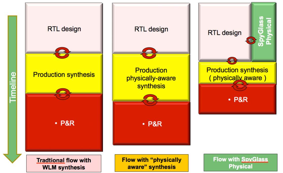
Using SpyGlass Physical during RTL design will slightly increase the time taken before RTL is ready for handoff. But the RTL will be of superior quality and so the synthesis and place & route will be much reduced, as will iterations back to fix RTL issues that manifest themselves as physical design issues such as routing congestion.


Consolidation and Competition: Who is Winning the $4.5 Billion Interface IP Race?