At TSMC’s Open Innovation Platform (OIP) Ecosystem Forum, Mentor made technical presentations on four different topics, two of them co-presented with TSMC and LSI Corporation. Those presentations are described below with links to downloadable pdf presentation files.
Finding and Fixing Double Patterning Errors in 20nm Design
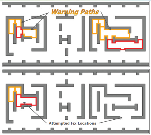
David also won the Customer’s Choice award (selected by attendee vote) for his presentation on Finding and Fixing Double Patterning Errors in 20nm Designs at TSMC’s Open Innovation Platform ecosystem event. In this presentation, David describes the new constraints that double patterning brings to the 20nm node, and how IC designers can deal with DP related design rule violations. View presentation…
A Platform for TSMC’s CoWoS 3DIC Reference Flow
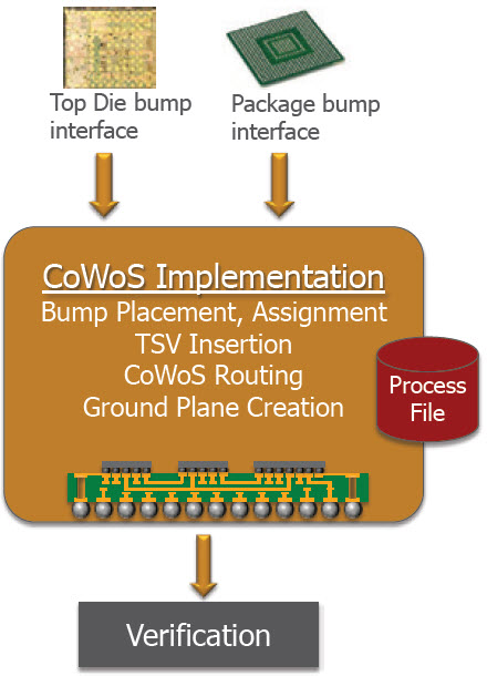
The first phase of 3DIC adoption will be based on silicon interposers. Designing multi-die systems using this technology introduces new challenges for the EDA design flow. At the TSMC OIP event, Mentor described solutions for 3DIC design specifically tailored to TSMC manufacturing processes.View presentation…
Automated Approach for Waiving Physical Verification Errors in IP
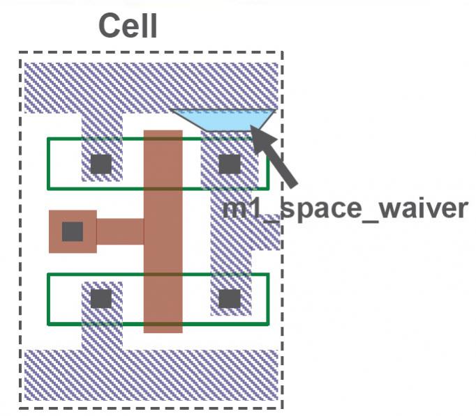
Redundantly reviewing recurring errors during custom and third-party IP integration can slow down SoC verification. An automated waiver management methodology enables design and verification teams to specify and process a variety of design rule waivers, reducing debugging time and improving SoC results. Mentor and LSI recently described the use of this technology at the TSMC OIP event. View presentation…
Improving IC Design for Reliability
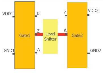
Verification of 20nm designs is expected to bring significant challenges. A robust verification methodology that addresses circuit reliability is increasingly difficult. At 20nm, new devices that incorporate thin oxides are less robust and more subject to electrical overstress (EOS) failures. The increased use of mixed-signal and multi-voltage design techniques also increases the likelihood that transistors could be implemented in an incorrect voltage domain. At TSMC’s recent OIP event, Mentor showed techniques to prevent long term electrical failure using new tools to validate ESD structures, protect against EOS, manage multiple power domains, and carefully balance sensitive analog circuits. View presentation…
Share this post via:


Comments
There are no comments yet.
You must register or log in to view/post comments.