




When I started in this business, we were at 3 micron HMOS. A few other things are close to that size. A red blood cells is about 9 microns, a human hair is about 100 microns. And in a bizarre “only in Japan” video, people compete to plane the thinnest shaving off a plank of wood. It turns out the answer is 9 microns. That’s a sharp blade!

Navigating the new patent landscape

If you are considering filing a patent, you should know about the new patent rules effectinve on March 16, 2013. Most importantly, patent rights will switch from “first-to-invent” to “first-to-file.” Before we continue, I am not a lawyer; I’m just a dumb blogger. Seek actual legal advice about the new patent laws if you think you might be affected.
As I understand it, the first-to-invent model worked basically like this: You invent rocket shoes on April 1, 2010 and start working on a patent application, which you file one month later. The guy next door you independently invents rocket shoes (what are the odds!) on April 10, 2010 and files a patent one week later. He got his patent application in first, but under first-to-invent, you, not your neighbor, might have the right to the patent. You would still, I assume, have the right to contest that application.
The new rules, which put the US in line with European, Canadian, and Japanese patent law, is “first-inventor-to-file.” Under this model, you should use those new rocket shoes to race to the patent office.
The America Invents Act makes changes to the definition of “prior art,” i.e., information that has been made available to the public that might be relevant to a patent’s claims of originality. So, if someone (say another of your terrible neighbors) describes your rocket shoes in a journal a day before you get to the patent office, her publication could have a bearing on your claim. In practice, this means that corporate lawyers will need to do much more diligent prior-art discovery.You should consult your legal advisor to understand these changes, and, as always, be careful about what you share publicly before filing for a patent.
The US patent office also now offers a fast track option that moves your application through in 1 year. Entrepreneurs and small businesses get a discount on the additional fast-track filing fee. In fact, the fee schedule changes as of March 19. All the fees are reduced, and there are two discount categories; one for small entities and one for ‘micro’ entities. There is no mention of ‘nano’ entities, so your tiny devices apparently have to pay full price…
Oh, and to reiterate: IANAL (I am not a lawyer) and this post should in no way be contrued as legal advice. In fact, the opinions set forth here are only my own and could be completely false (like the idea that those rocket shoes would actually work). If you actually attempt to navigate the incredibly complex world of patent law based on this blog, and you fail, it’s your own dumb fault. If you plan to file a patent, go see a lawyer for goodness sake.
Apple and Samsung Do It Again

The numbers are starting to come in for how everyone did in Q4. According to Cannacord Genuity, Apple made 69% of the profit and Samsung made 34%. What do you notice about those numbers? They add up to more than 100%. HTC supposedly made 1% of the profit and everyone else either broke even or lost money. Basically Apple and Samsung have rendered everyone else in the market irrelevant and pretty much doomed to run out of money.
In terms of smartphone units, IDC’s numbers have Samsung at #1 with 63.7M units (up 70% on last year), Apple is #2 with 47.89M and a surprising #3, admittedly a long way behind, is Huawei with 10.8M.
Surprisingly, Google’s Android, which accounts for about 70% of smartphone activations, is completely dominated by Samsung when it comes to making any money. How long all the other Android players can continue without making any profit remains to be seen. Google’s own Motorola is losing money still, and it will be interesting to see what they bring to market this year since they claim that the existing product pipeline is now flushed and so future products should be ones designed after the Google acquisition of Motorola Mobility. It will also be interesting to see if Google keeps the Android playing field level or gives Motorola Mobility something that Samsung doesn’t get its hands on so quickly.
Also worryingly for Google, Samsung has a third operating system Tizen that it is just starting to bring to market. This is the metamorphosis of project Meego that Samsung took over when Nokia dropped it to focus on its Microsoft strategy (how’s that working, by the way?). Since carriers apparently would really like a 3rd ecosystem to keep Apple and Google off-balance, it will almost certainly be successful. For sure Microsoft/Nokia is not that third ecosystem and, while the recently renamed Blackberry (the company used to be called Research In Motion or RIM) has just come out with a brand-new version of their operating system, it seems unlikely to do more than shore them up inside major corporate strongholds such as government and some huge companies.
Tablets are big. So big that many people are predicting that in 2013 tablets will outsell notebooks and desktop PCs. According to Canalys, Apple sold 22.9 million tablets for 49% share, Samsung sold 7.6 million, Amazon sold 4.6 million tablets, and Google’s Nexuses sold 2.6 million. What will happen to the tablet market is going to be interesting. Amazon presumably sells its tablets close to their cost and makes it up on other revenue streams. Apple, which certainly isn’t selling anything like near cost, also has other revenue streams of content. Embarrassingly for Google, Amazon is selling more Android tablets than they are despite Google’s strategy of flooding the market with cheap tablets and making the money on search and other monetization schemes. Amazon is flooding better. Samsung is doing fine for now but could get squeezed since it has a pure hardware business, at least for now.
Tubes of the Future

So what is a silicon nanowire? It is basically a FET where the active element is a wire 3-20nm in diameter. So where a FinFET has the gate wrapped around 3 sides of the transistor, a nanowire (NW) has it wrapped around all four. In essence, the wire runs through the middle of the gate.
There seem to be three issues about building a silicon nanowire. First, suspending the wire above the substrate, then depositing the gate around the wire, and controlling the shape of the wire (you’d like it to be as circular as possible). One thing you can do with NW that is new is to run several wires through the same gate, either to switch multiple signals simultaneously or to get higher current.
Beyond 7nm, silicon is not the ideal substance for nanowires and it is better to use carbon nanotubes. A carbon nanotube FET (CNTFET) has much higher currents compared to silicon. This has the potential of an enormous increase of 3-10X in power and/or performance. Carbon nanotubes are a roll of carbon 1nm in diameter. The bandgap can be adjusted which means we can have both normally-on and normally-off transistors (like “p” and “n” type transistors in CMOS) and so we can continue to use complementary logic.
The fabrication process is completely different than for silicon NW. The carbon nanotubes are created as a sort of raw material away from the wafer fab. One issue is that some percentage of them are metallic rather than semiconducting and so repeated purification steps via column chromatography are required to ensure that (almost) none of the metallic ones get through.
The carbon nanotubes are then laid onto the wafer in a single layer at 6nm spacing. Using cut masks these can then be patterned.
One big challenge to be solved with CNT is that currently we don’t have a good way to contact to them without requiring an extremely long (say 300nm) contact area. This will need a lot of work to solve to make CNT practical.
ARMs in the Clouds
The most interesting session at the Linley Tech Data Center Conference last week was the last one, on Designing Power Efficient Servers. What this was really about was whether ARM would have any success in the server market and what Intel’s response might be.
Datacenters are now very focused on power efficiency and many track Power Usage Efficiency (PUE) which is the ratio of the power used by the servers to the power used by everything else (routers, cooling, power distribution, backup etc). 2 is average and new facilities target 1.5. Power is generally the limiting factor on the size of a rack and the size of a datacenter so further improvements are required. More than a third of the cost of ownership of a datacenter is proportional to the electrical usage. So despite the obvious issues with a change of architecture (porting software), if big savings can be made they can be truly compelling.
Historically, server processors focus on complex highly-superscalar CPUs designed for the best possible single thread performance. But all that instruction reordering wastes power as does very long pipelines and high clock rates. For many datacenters focused on heavy computation this is the right type of server. But many other datacenters are focused on highly threaded workloads that can easily take advantage of more cores per chip/server/rack. There are also opportunities to integrate high-speed I/O and networking all on the same chip.
The obvious beneficiary of this means of thinking is ARM. They announced the 64-bit Cortex-A57 (no, I don’t understand ARM’s numbering system either) focused on this opportunity. Intel has responded with Centerton which is their first server processor based on Atom. But, as Linley pointed out, it only has the same level of integration as Xeon and so requires external USB, Ethernet, disk controllers etc. TDP is 6.3W at 1.6GHz which looks nice until you consider that its performance is so much lower than Xeon and, in fact, it is less power efficient than Xeon. Intel’s next generation will be Avoton (no, I don’t understand Intel’s naming system either) in 22nm with second generation Atom architecture and “integrated system fabric.” But details have not yet been announced.
So who are working on alternatives? Tilera has repurposed their massively multicore processor for cloud servers. Calxeda is shipping an ARM-based server processor. AppliedMicro and Cavium are developing 64-bit ARM CPUs and AMD has announced that it will use the Cortex-A57 in 2014 server products.
Calxeda presented their roadmap. Today they can put 3,000 servers in a single rack with 12,000 cores, 12TB DRAM, power requirements down by 90%, eliminating 9 miles of cabling and 125 ethernet switches. That’s the sort of thing that will get the attention of Google, Facebook and Amazon.
They had an interesting example: server capacity to service 10,000,000 HTTP requires per second on a 1Gb network infrastructure. The densest x86 solution requires 1997 servers on 4 racks with 44 switches and consumes 37kW. Using Calxeda’s ARM-based SoCs, this is 1535 servers on 1.6 racks with 2 switches and 13kW of power. 40% lower TCO, 61% less space, 95% fewer switches, 65% less energy. Close to their elevator pitch: 1/10th of the energy in 1/10th of the space and 1/2 the TCO and all the performance.
AppliedMicro had a similar message. There are computationally intensive workloads such as high-frequency trading or data-mining. But many cloud workloads are not like that and can take advantage of lots more cores even if the scalar performance of each one is not the maximum. Their X-Gene microserver integrates network, I/O and storage all on one chip.
They have their comparison example too. A traditional server architecture providing 2560 cores requires 160 nodes, 28kW in 2 racks. With X-Gene, the same 2560 cores just requires 320 nodes, 19kW in 1 rack. So half the size and half the power.
The server processor market is about $10B today so it is a prize worth fighting over. And, unlike the smartphone processor market, the major players are not designing their own SoCs so the whole market is available for merchant suppliers.
Notes from Common Platform: Collaborate or Die

FinFETs are hot, carbon nanotubes are cool, and collaboration is the key to continued semiconductor scaling. These were the main messages at the 2013 Common Platform Technology Forum in Santa Clara.
The collaboration message ran through most presenations, like the afternoon talk by Subi Kengeri of GLOBALFOUNDRIES and Joe Sawicki of Mentor Graphics.
Subi talked about technology development, identifying the market drivers of technology (mobile), the technology challenges (power density, metrology for FinFETs), and the future device architectures (III-V, SiGe, carbon tube). Listening to him lay out the technology landscape, one starts to understand why cooperation between Common Platform Alliance members (IBM, Samsung, GlobalFoundries) is so important.
While the industry was once full of vertically integrated semiconductor companies who could conceive of, design, and manufacture their ICs under one roof (“real men have fabs”), today, the fabless semiconductor industry depends on the “ecosystem” of IP, EDA, manufacturing, test and packaging. The EDA part of the equation, design enablement and manufacturing ramp, was covered by Joe Sawicki.
Joe emphasized that DFM today involves pulling manufacturing knowledge into the design flow as early as possible. Mentor is keenly aware of the importance of manufacturing on all stages of design, so much so that they built a new website focused on foundry solutions.
To get a manufacturable design, you have to go far beyond simply reading in a technology file with basic spacing rules. You need enough information flowing between tools for a true design/manufacturing co-optimization. From the EDA point of view, this means merging physical verification with place & route (Calibre InRoute), fusing DFM with test and yield analysis, streamlining final verification (pattern matching, DFM scoring), improving metal fill, developing technologies to improve circuit reliability (PERC), and improving test coverage for low- or 0-defect applications (cell-aware ATPG). It begins to look as if the nice, distinct boxes of the IC design flow are escaping their boundaries, blending together. Is it chaos? Is it cats and dogs living together? No, it’s the future; everything working better through mashups and collaborations.
In fact, my analysis of word usage in the day’s presenatations revealed that “collaboration” was the most frequently used term of the day. Keep in mind that this reporter’s analysis is based on general recollections during happy hour, but still, I stand by it.
No EUV before 7nm?

I was at the Common Platform Technology Forum this week. One of the most interesting sessions is IBM’s Gary Patton giving an overview of the state of semiconductor fabrication. Then, at lunchtime, he is one of the people that the press can question. In this post, I’m going to focus on Extreme Ultra-Violet (EUV) lithography.
You probably know that the biggest challenge is the light source. This is actually made with droplets of tin. One laser shapes the drop and then another high powered laser zaps the drop to create plasma and EUV light. This is collected, goes through 6 mirrors with very low efficiency and a reflective mask. Very little, maybe 5%, of the original light actually makes it to the wafer to expose the photoresist. Right now the power of the light source is up to about 30W but it needs to be more like 250W and so it is off by a factor of 10.
Gary also mentioned two other problems that I’ve written about before but which don’t get mentioned nearly so much. After all, these are only problems if we get a usable EUV light source that works reliably ten billion times a day with adequate power.
The two other problems are that masks will not be defect free and that it is not possible to put a pellicle on the mask (since it would absorb all the EUV).
First, the defect problem. There are two issues. Firstly, the mask will have defects that will print and so either the design needs to be redundant enough that it doesn’t matter or else the defects need to be on parts of the mask that don’t matter since they are going to print anyway. This means knowing where the defects are and that is the next problem. You can’t just look for them with visible light since they are too small. So you need to scan them. But the scale of a mask versus the scale of a defect is huge: it is equivalent to searching 10% of California to make sure there are no golf balls there.
In refractive optics (what we use today) the mask is covered with a thin transparent film called a pellicle. One purpose of the pellicle is that any contamination that would end up on the mask instead ends up on the pellicle. It is thus out of the focal plane of the stepper and so doesn’t print. EUV masks cannot have a pellicle. But that means that any contamination will print. Worse, it won’t be obvious that this his happening and it will continue to print until the mask is cleaned. This is potentially very expensive since hundreds more fabrication steps may take place on a wafer that is actually already a dud. The whole wafer. Every die.
Some people have said that getting EUV to work is “just engineering.” Gary says this is not the case. “It is not just hard engineering work, it is hard physics problems too.” At lunch someone asked Gary if it was like 80% engineering with 20% of physics problems to be resolved. He said he wasn’t really sure how you put a number on it like that but his guess would be 60% physics problems and 40% engineering.
If EUV becomes workable, IBM thinks that it will be for the 7nm node. Not 14nm or 10nm. It seems that “EUV will eventually work because it has to.” But reality doesn’t always cooperate on that basis.
Using Soft IP and Not Getting Burned

The most exciting EDA + Semi IP company that I ever worked at was Silicon Compilers in the 1980’s because it allowed you to start with a concept then implement to physical layout using a library of parameterized IP, the big problem was verifying that all of the IP combinations were in fact correct. Speed forward to today and our industry still faces the same dilemas, how do you assemble a new SoC designed with hard and soft IP, and know that it will be functionally and physically correct?
They say that it takes a village to raise a child, so then in our SoC world it takes collaboration between Foundry, IP providers and EDA vendors to raise a product. One such collaboration is between:
- TSMC with their Soft IP alliance program
- An Atrenta IP Kit
- Sonics has developed Soft IPusing Atrenta and TSMC
These three companies are hosting a webinar on Tuesday, March 5, 2013 at 9AM, Pacific time to openly discuss how they work together to ensure that you can design SoCs with Soft IP and not get burned.
Agenda
- Moderator opening remarks
Daniel Nenni (SemiWiki) (5 min) - The TSMC Soft IP Alliance Program – structure, goals and results
(Dan Kochpatcharin, TSMC) (10 min) - Implementing the program with the Atrenta IP Kit
(Mike Gianfagna, Atrenta) (10 min) - Practical results of program participation
(John Bainbridge, Sonics) (10 min) - Questions from the audience (10 min)
Speakers
Daniel Nenni
Founder, SemiWiki
Daniel has worked in Silicon Valley for the past 28 years with computer manufacturers, electronic design automation software, and semiconductor intellectual property companies. Currently Daniel is a Strategic Foundry Relationship Expert for companies wishing to partner with TSMC, UMC, SMIC, Global Foundries, and their top customers. Daniel’s latest passion is the Semiconductor Wiki Project (www.SemiWiki.com).
John Bainbridge
Staff Technologist, CTO office, Sonics, Inc.
John joined Sonics in 2010, working on System IP, leveraging his expertise in the efficient implementation of system architecture. Prior to that John spent 7 years as a founder and the Chief Technology Officer at Silistix commercializing NoC architectures based upon a breakthrough synthesis technology that generated self-timed on-chip interconnect networks. Prior to founding Silistix, John was a research fellow in the Department of Computer Science at the University of Manchester, UK where he received his PhD in 2000 for work on Asynchronous System-on-Chip Interconnect.
Mike Gianfagna
Vice President, Corporate Marketing, Atrenta
Mike Gianfagna’s career spans 3 decades in semiconductor and EDA. Most recently, Mike was vice president of Design Business at Brion Technologies, an ASML company. Prior to that, he was president and CEO for Aprio Technologies, a venture funded design for manufacturability company. Prior to Aprio, Mike was vice president of marketing for eSilicon Corporation, a leading custom chip provider. Mike has also held senior executive positions at Cadence Design Systems and Zycad Corporation. His career began at RCA Solid State, where he was part of the team that launched the company’s ASIC business in the early 1980’s. He has also held senior management positions at General Electric and Harris Semiconductor (now Intersil). Mike holds a BS/EE from New York University and an MS/EE from Rutgers University.
Dan Kochpatcharin
Deputy Director IP Portfolio Marketing, TSMC
Dan is responsible for overall IP marketing as well as managing the company IP Alliance partner program.
Prior to joining TSMC, Dan spent more than 10 years at Chartered Semiconductor where he held a number of management positions including Director of Platform Alliance, Director of eBusiness, Director of Design Services, and Director of Americas Marketing. He has also worked at Aspec Technology and LSI Logic, where he managed various engineering functions.
Dan holds a Bachelor of Science degree in electrical engineering from UC Santa Barbara, a Master of Science in computer engineering, and an MBA from Santa Clara University.
Registration
Sign up here.
Semiconductors Down 2.7% in 2012, May Grow 7.5% in 2013
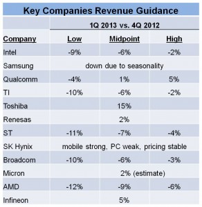
The world semiconductor market in 2012 was $292 billion – down 2.7% from $300 billion in 2011, according to WSTS. The 2012 decline followed a slight gain of 0.4% in 2011. Fourth quarter 2012 was down 0.3% from third quarter. The first quarter of the 2013 will likely show a decline from 4Q 2012 based on typical seasonal patterns and the revenue guidance of key semiconductor companies.
Intel, Texas Instruments (TI), STMicroelectronics (ST), and Broadcom all have similar guidance – with the low end ranging from declines of 9% to 11%, the midpoint a 6% or 7% decline, and the high end a decline of 2% to 4%. AMD’s guidance is slightly more negative, ranging from -12% to -6%. Qualcomm, Toshiba, Renesas Electronics and Infineon expect 1Q 2013 revenues to increase from 4Q 2012, ranging from Qualcomm’s midpoint of 1% to Toshiba’s 15% guidance for its Electronics Devices segment. The major memory companies did not give specific guidance. Samsung expects a seasonal decline. SK Hynix sees strong demand for mobile applications but weak demand for PC applications. We at Semiconductor Intelligence estimate a 2% increase for Micron Technology based on its projections of bit growth and price trends. We estimate the overall semiconductor market will decline 1% to 3% in 1Q 2013.
What is the outlook for the years 2013 and 2014? The latest economic forecast from the International Monetary Fund (IMF) calls for World real GDP growth to accelerate from 3.2% in 2012 to 3.5% in 2013 and 4.1% in 2014. U.S. GDP growth is expected to slow slightly from 2.2% growth in 2012 to 2.0% in 2013 before accelerating to 3.0% in 2014. The Euro Area will continue to work through its debt crisis in 2013 with a GDP decline of 0.2% in 2013 and then recover to 1.0% growth in 2014. Japan’s GDP declined 0.6% in 2011 due to the devastating earthquake and tsunami. Rebuilding boosted Japan’s GDP 2.0% in 2012, but growth is expected to moderate to 1.2% in 2013 and 0.7% in 2014. Asia will continue to be the major driver of World economic growth. China’s GDP is forecast to accelerate from 7.8% in 2012 to 8.2% in 2013 and 8.5% in 2014. The IMF groups South Korea, Taiwan, Singapore and Hong Kong in the category of Newly Industrialized Asia (NIA). NIA GDP growth should pick up from 1.8% in 2012 to 3.2% in 2013 and 3.9% in 2014.
Semiconductor market growth is closely correlated to GDP growth. Our proprietary model at Semiconductor Intelligence uses the GDP growth rate and the change in GDP growth rate (acceleration or deceleration) to predict semiconductor market growth. Other major factors in determining semiconductor market growth are key electronic equipment drivers (such as media tablets and smartphones), inventory levels, fab utilization and semiconductor capital spending. Our prior forecast in November 2012 called for 9% semiconductor market growth in 2013 and 12% growth in 2014. Based on the slight decline in the market in 4Q 2012 and expected decline in 1Q 2013, we have revised the 2012 forecast to 7.5%. We are holding our 2014 forecast at 12%. The chart below compares our forecast with other recent forecasts for 2013 and (where available) 2014.
At the low end of the 2013 forecasts are WSTS and Gartner at 4.5% and IDC at 4.9%. Mike Cowan’s January model adjusted to the final 2012 data yields a forecast of 6.1%. IHS iSuppli is the highest at 8.3%, slightly higher than our 7.5%. The available forecasts for 2014 are 5.2% from WSTS, 9.9% from Gartner and 12% from Semiconductor Intelligence. Gartner and Semiconductor Intelligence both show significant growth acceleration from 2013 to 2014 while WSTS has only slight acceleration.
***
Semiconductor Intelligence does consulting and custom market & company analysis. See our website at:
http://www.semiconductorintelligence.com/
RTL Clock Gating Analysis Cuts Power by 20% in AMD Chip!
Approximately 25% of SemiWiki traffic originates from search engines and the key search terms are telling. Since the beginning of SemiWiki, “low power design” has been one of the top searches. This is understandable since the mobile market has been leading us down the path to fame and fortune. Clearly lowering the power consumption of consumer products and networking centers is an important design consideration and this effort begins with the chips used in these devices.
Semiconductor design innovators like AMD wanted to improve on previous generation designs in terms of faster performance in a given power envelope, higher frequency at a given voltage, and improved power efficiency through clock gating and unit redesign.
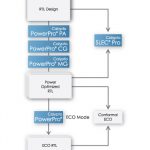
The AMD low-power core design team used a power analysis solution (PowerPro[SUP]®[/SUP] from Calypto[SUP]®[/SUP]) that helped analyze pre-synthesis RTL clock-gating quality, find opportunities for improvements, and generate reports that the engineering team could use to decrease the operating power of the design.
By targeting pre-synthesis RTL, power analysis can be run more often and over a larger number of simulation cycles — more quickly and with fewer machine resources than tools that rely on synthesized gates. The focus on clock gating and the quick turnaround of RTL analysis allowed AMD to achieve measurable power reductions for typical applications of a new, low-power X86 AMD core.
This article by Steve Kommrusch of AMD describes the power analysis methodology AMD used to improve clock-gating efficiency and identify key features and advantages that the tool delivered. Quantitative results are interpreted and presented in graphs and tables. Comparative data between PowerPro results and PTPX post-synthesis results, show that doing power analysis at the RTL stage rather than waiting until post-gate synthesis was very useful.
Ultimately, even given instructions per clock (IPC) and frequency improvements, PowerPro helped achieve an approximately 20% reduction in typical dynamic application power compared to an already-tuned low-power X86 CPU. You can read the whole article HERE.
Calypto Design Systems leads the industry in technologies for ESL hardware design and RTL power optimization. These technologies empower designers to create high quality and low power electronic systems for today’s most innovative electronic products.