Bronco Webinar 800x100 1

Synopsys Magma Acquisition Stock Trading Under Investigation?

Synopsys Magma Acquisition Stock Trading Under Investigation?
by Daniel Nenni on 02-12-2013 at 7:00 pm

An attorney from the Division of Enforcement at the U.S. Securities & Exchange Commission contacted me in regards to activity on SemiWiki. Not a great way to start a Monday! Given the parameters of the discussion and the type of questions it is undoubtedly (in my humble opinion) concerning the Synopsys acquisition of Magma.

This conversation and the resulting heart palpitations give ample support to John Cooley’s decision to keep DeepChip.com a “dumb” HTML site. SemiWiki, on the other hand, is an “intelligent” site built on a relational database with a content management system enabling full social media capabilities, data mining, and analytics.

The capability in question here is SemiWiki’s private email where registered members can talk amongst themselves under the cover of their screen names. SemiWiki respects the privacy of our members and will never willingly disclose member information. You can shine bright lights in our eyes and waterboard us, we are not talking. A subpoena by the Federal Government however is a completely different story.

Why would people commit felonies on SemiWiki or any other social media site under the guise of anonymity? The same reason why politicians tweet their private parts, why people post their crimes on FaceBook, and why movie stars and famous athletes send incriminating emails and texts. Because they think they are clever but they are not.

The most recent one that comes to mind is former four star General and CIA Director David Petraeus who communicated with his mistress via draft emails on a gmail account where no emails were actually sent. Clever right? Apparently not as the deleted draft emails were “discovered” during the investigation. Bottom line, digital footprints leave tracks that cannot be covered no matter how clever you think you are, believe it.

The other interesting aspect of this story is Frank Quatrone. From a previous blog “Synopsys Eats Magma…”:

Investment banker Frank Quattrone, formerly of Credit Suisse First Boston (CSFB), took dozens of technology companies public including Netscape, Cisco, Amazon.com, and coincidentally Magma Design Automation. Unfortunately CSFB got on the wrong side of the SEC by using supposedly neutral CSFB equity research analysts to promote technology stocks in concert with the CSFB Technology Group headed by Frank Quattrone. Frank was also prosecuted personally for interfering with a government probe.

To make a long story short: Frank Quattrone went to trial twice: the first ended in a hung jury in 2003 and the second resulted in a conviction for obstruction of justice and witness tampering in 2004. Frank was sentenced to 1.5 years in prison before an appeals court reversed the conviction. Prosecutors agreed to drop the complaint a year later. Frank didn’t pay a fine, serve time in prison, nor did he admit wrongdoing! Talk about a clean getaway! Quattrone is now head of merchant banking firm Qatalyst Partners, which, coincidently, handled the Synopsys acquisition of Magma on behalf of Magma.

A conspiracy theorist might think that the Federal Government is keeping an extra close eye on Frank hoping to rid themselves of the black eye he gave them last time around. I’m not a conspiracy theorist so I really wouldn’t know.

I’m including this disclaimer again since it apparently made the legal folks from the SEC chuckle:

Disclosure: This blog is opinion, conjecture, rumor, and non legally binding nonsense from an internationally recognized industry blogger who does not know any better. To be clear, this blog is for entertainment purposes only.


Video? Tensilica Has You Covered

Video? Tensilica Has You Covered
by Paul McLellan on 02-12-2013 at 2:01 am

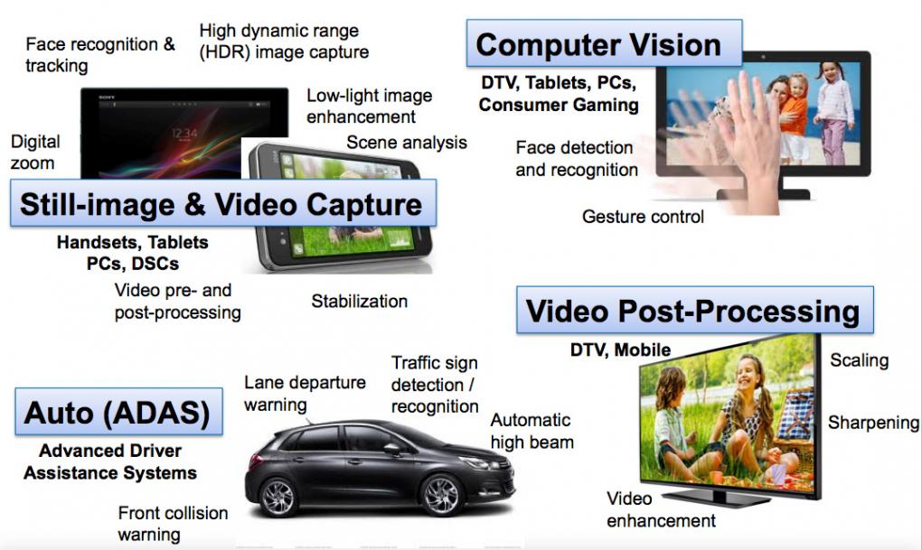
Video is a huge growing area and advanced imaging applications are becoming ubiquitous. By “advanced” I mean more than just things like cameras in your smartphone. There is lots more coming, from high-dynamic range (HDR) photography, gesture recognition, more and more intelligent video in cars to keep us safe, face-recognition and so on. And not at the resolutions that we are used to, things are going ultra-high definition (UHD) with 4Kx2K pixels, 18 megapixel cameras (in our phones). Result, video processing requirements are doubling every 18 months whereas Moore’s law is doubling more like every 3 years these days.

So what’s a designer to do? The application processor chip in a smartphone already has some cores, can’t we use them? It probably had a dual/quad core ARM Cortex of some sort. It probably has a dual or quad core GPU, maybe from Imagination. It probably already has some specialized video circuitry such as H.264 encode and decode. Isn’t that enough? Even ignoring power this is not enough processing performance for many of these new applications. With a realistic power limit it is not even close. Video didn’t just kill the radio-star, it is killing the power budget too.

First the ARM. High-resolution video processing requires at least 4 cores but at 1.5GHz that is 3W, which is about 10 times the power budget. But at least it is easy to program. If we try and use the GPU for the image processing, it is not a very good match since the GPU is focused on floating point and 3D graphics. Plus GPUs are notoriously hard to program for anything other than the graphics pipeline for games etc. Using dedicated hardware can work well for anything like codecs where the standards are fixed (for a decade or so) but the new application areas are in flux with the algorithms changing all the time. And while adding a couple of specialized blocks can be attractive compared to using that ARM, the tradeoff doesn’t look so good once you get up to a dozen or more blocks. They take up a lot of area and consume a lot of power.


Today Tensilica is announcing their Imaging Video Processor (IVP) family and the first member of the family. Of course under the hood this is built on top of the Xtensa VLIW processor generation technology and the associated software technology (vectorizing compilers, modeling etc) that go with it. So while the video aspects are new the fundamental technology is mature.

Of course the focus is on low-power handheld devices since these have the most severe constraints: low power budgets, consumer price points and product cycles. The IVP hits the sweet spot between ease of programming and energy efficiency.


The core is licensable but that’s not all there is. RTL, EDA scripts, Instruction-set simulator, IDE (Eclipse-based), C compiler, debugger, image processing applications, operating systems, documentation. And software partners with deep video expertise who work on the bleeding edge of video algorithms.

In the crucial measure of 16b pixel operations per second per watt, IVP is about 10 to 20X as efficient as using the ARM Cortex, and about 3 to 6X as efficient as using the GPU. All with the programming flexibility of a software implementation, a big advantage over direct implementation in RTL in an area where tweaks to algorithms and even entirely new algorithms are commonplace.

Oh, and there is an FPGA development platform too, so that you can hook up an IVP to cameras, TVs, screens or whatever.

Tensilica will be showing the new product in Barcelona at Mobile World Congress at the end of the month. They are in Hall 6 at booth D101. If you are lucky enough to be in Barcelona, one of my favorite European cities, then go by and see them. And don’t miss all the amazing Gaudi architecture. Or the Miro museum. And tapas on la Rambla.

More details on Tensilica’s website here.


Assertion Synthesis: Atrenta, Cadence and AMD Tell All

Assertion Synthesis: Atrenta, Cadence and AMD Tell All
by Paul McLellan on 02-11-2013 at 6:22 pm

Assertion Synthesis is a new tool for verification and design engineers that can be used with simulation or emulation. At DVCon Yuan Lu of Atrenta is presenting a tutorial on Atrenta’s BugScope along with John Henri Jr of Cadence explaining how it helps emulation and Baosheng Wang of AMD discussing their experiences of the product.

Creating an adequate number of high quality assertions and coverage properties is a challenge in any verification plan. Assertion Synthesis takes as input the RTL description of the design and its test environment and automatically generates high quality whitebox assertions and coverage properties in standard language formats such as SVA, PSL and Verilog. Assertion Synthesis enables an automated assertion-based verification methodology that improves design quality and reduces verification overhead.

Here’s the 5000ft version of what Assertion Synthesis is. BugScope watches the simulation (or emulation, which I think of as a special sort of simulation) of the design and observes its behavior. Based on what it sees, BugScope automatically generates syntactically correct assertions about the design, behaviors that it believes are always true based on the simulation.

The designer and verification engineers can use these assertions in three different ways:

[LIST=1]

  • They agree with BugScope that the assertion should always be true. There is now a new assertion that can be used in subsequent verification runs that is ready for use. Construction of syntactically correct assertions can take hours so this is a real time saver. Of course, once included in the verification run, the assertion will trigger anytime the condition is violated making it easy to track down the newly introduced problem.
  • The assertion should not always be true. But this means that there are not enough simulation vectors to exhibit to BugScope any situation in which it is actually not true. This is a real coverage hole and more vectors are required. This is obviously also very useful information.
  • The assertion is indicating a behavior that should, in fact, never happen. BugScope has identified a real design issue, something it considers should happen that the designer knows should not.

    All three of these alternatives result in an improved verification process: either more assertions added very cheaply, a coverage hole identified, or a real error in the design.

    The DVCon tutorial, which is officially titled Achieving Visibility into the Functional Verification Process using Assertion Synthesis, is on Thursday February 28th from 1.30pm to 5pm in the Donner Ballroom. More details are here.


  • Magic? No! It’s Computational Lithography

    Magic? No! It’s Computational Lithography
    by Beth Martin on 02-11-2013 at 7:00 am

    The industry plans to use 193nm light at the 20nm, 14nm, and 10nm nodes. Amazing, no? There is no magic wand; scientists have been hard at work developing computational lithography techniques that can pull one more rabbit out of the optical lithography hat.

    Tortured metaphors aside, the goal for the post-tapeout flow is the same as always – to compensate for image errors on the wafer due to diffraction or process effects. Resolution enhancement technology (RET) and optical proximity correction (OPC) do this by moving edges and adding sub-resolution shapes to the pattern that will be written to the photomask.

    Now, if you are prepared to have your mind blown by new computational lithography techniques, you can sign up for the SPIE Advanced Lithography conference. There is so much going on with computational lithography that I couldn’t start to cover it all here. I’ll introduce two presentations on my list: “Inverse lithography technique (ILT) for advanced CMOS nodes,” by scientists from ST Microelectronics and Mentor Graphics, and “Effective model-based SRAF placement for full-chip 2D layouts” by Mentor Graphics R&D. In both of them, the authors address the problem of lithographic hotspots that can remain after full-chip OPC. Without innovations like those described in these papers, such as the litho quality benefits of free–form SRAF placement, the solution would be to tune your OPC recipe to address each hotspot and maybe, eventually, fix them all. This is not a very good solution.

    A better way is to use a more aggressive correction approach to solve just the hotspots that remain after traditional OPC/SRAF insertion, and then stitch the result back into the OPC-ed full-chip layout. Inverse lithography technology is so called because rather than moving the fragmented edges of the starting (target) shapes to produce the desired wafer image, it uses a rigorous mathematical approach to solve an inverse problem, thus generating the “ideal output mask (OPC + SRAF) shapes” that will result in the desired image on the wafer. ILT solves an optimization problem, and as such is computationally expensive if applied full-chip. At SPIE, the authors present it as a tool for localized printability enhancement (LPE).

    This chart shows their iterative localized printability enhancement flow.
    You first perform OPC and SRAF insertion. Verification then gives you a list of hotspots and you apply ILT only to those hotspots. The research presented uses Mentor’s ILT engine (called pxOPC) plus some automation to cut and stitch the repaired areas back into the full layout.

    Author Alex Tritchkov of Mentor Graphics told me that with their inverse lithography technology, the OPC and the SRAFs have greater degrees of freedom and can employ non-intuitive but manufacturable shapes. This allows for significant process window improvement for certain critical patterns, which are very hard to achieve with conventional OPC/SRAF insertion.

    Tritchkov sees ILT as useful both during R&D when design rules are not established, the OPC/RET recipes are immature, and the test chips are pushing the resolution limits, but also in high-volume production to eliminate rework and reduce cost and risk. Papers 8683-14 and 8683-17 will be presented on Tuesday, 26 February at 3:50pm and 4:50pm, respectively.

    Registerfor SPIE today.


    Want 10nm Wafers? That’ll Cost You

    Want 10nm Wafers? That’ll Cost You
    by Paul McLellan on 02-10-2013 at 9:01 pm

    As you know, I’ve been a bit of a bear about what is happening to wafer costs at 20nm and below. At the Common Platform Technology Forum last week there were a number of people talking about this in presentations and at Harvey Jones’s “fireside chat”.

    At the press lunch I asked about this. There are obviously lots of technical issues to address to get to 10nm and below, and I don’t want to underestimate them, but at some point an important question is “at what cost.” Historically, with each process generation we have had something like a 50% reduction due to scaling along with a 15% increase in wafer fabrication cost resulting in an overall 35% reduction in cost per transistor.

    Mike Noonen of Global Foundries answered the question. But like that dog in Sherlock Holmes that didn’t bark, Mike didn’t say the costs are going down. He talked about the value of moving to more advanced process nodes: higher performance, lower power. This is all true, of course, and for some markets the value is enormous (smart phones and data center servers most obviously). However, we are clearly entering a new era where we don’t get everything for free anymore. Nobody knows what will happen to Moore’s law in practice when we don’t get more transistors, faster designs, lower power designs, and it’s all cheaper. Instead, it is “how much extra would you pay for lower power?”.

    Later, Gary Patten of IBM was more explicit. “Yes,” he said, “there is a cost benefit but it is much smaller that we have been used to.”


    The problem is lithography (see the picture, litho is on the right). Even the purple bar on the right, which is EUV, doesn’t really get those costs completely under control.

    In Handel Jones’s fireside chat with Brian Fuller, he said that they have done significant work to show a reduction in cost. He said that the big issue is parametric yield, mostly related to leakage. Some yield is driven by defects in processing and, while there is always some learning to be done, that is under control. But at these advanced nodes, with high variability, the issue of yield needs to be optimized at the design stage or parametric yield loss will make render the design financially non-viable.

    Handel reckoned that design closure costs doubled from 45nm to 28nm and are double again from 28nm to 20nm. Leakage is the killer and the designs need to be optimized for it.

    The other challenge at these advanced nodes is the volume required to make a design economic. Handel’s numbers are a cost of $100M/design at 20nm meaning a market of $1B or more for that design. Only 4 or 5 companies (Apple, Samsung, Intel…) can cope with this but the volumes will be very high.

    Even Intel is not immune. At the press lunch someone pointed out that Intel’s costs had gone up 30% from 32nm to 22nm and it had taken them 24 months to get them down and under control. And of course, they play in a market with very high margins and where performance is valued very highly. That won’t work for more cost-sensitive markets.

    If you read articles about electronics in the non-specialist press (aka newspapers, Time, the Economist etc) everyone assumes that electronics is going to continue getting cheaper. But we may be in a different regime. Yes, your smartphone will have longer battery life and do amazing voice recognition and so on. But it won’t get much cheaper than it is today (today meaning that most of the expensive components are manufactured on 28nm). But wait, it gets worse. If all that voice recognition requires twice as many transistors for all those processor cores then the cost of that chip may be close to twice as much as the old one. This is not what we are used to.


    Cadence Sigrity, Together At Last

    Cadence Sigrity, Together At Last
    by Paul McLellan on 02-10-2013 at 9:00 pm

    In July Cadence acquired Sigrity, one of the leaders in PCB and IC packaging analysis. Until a decade ago, signal integrity and power analysis was something that only IC designers needed to worry about. For all except the highest performance boards, relatively simple tools were sufficient. Provided you hooked up the pins on all the packages correctly then the design would work. That is no longer the case and for this reason Sigrity created their product line and subsequently Cadence acquired them.

    When I was at Cadence we acquired Cadmos, who were the leader in IC signal integrity at the time. One of the challenges with an acquisitions like Cadmos and Sigrity is that there are really two things involved: a running business and a core technology. Going forward, two things need to be done: ramp up the running business, and integrate the core technology into other existing products. The reason that it is such a challenge is that there is only one team in place that understands the product well enough to do these things, and they are stretched thin to do both. Although it is still work-in-progress, Cadence have come a long way to getting the Sigrity products integrated into Allegro.


    By November, Cadence had the Sigrity tools (Power Aware SI, Serial Link SI, Power Integrity, and Package Extraction) updated with Cadence look and feel and available through standard Cadence contracts. Now, in January, Cadence has Sigrity integrated into their high-end Allegro board design suite so that Sigrity products can be used directly from within the Allegro environment.

    Capabilities to address something like signal integrity typically show up first as verification tools to check a design has no problems, and allowing the designer to manually fix up the handful of things that get identified. The trouble is that design constraints never get any easier and so verification on its own is not enough. When it is no longer a handful of things that get identified as problems but hundreds or thousands then the technology needs to get integrated into the core algorithms to enable constraint-based design. It is no longer good enough to identify problems, it is necessary to avoid creating them in the first place.


    The most critical and highest speed signals on a board these days are typically high-speed serial links. These run at multi-gigabit/s speeds, fast enough to require special analysis that almost goes back to Maxwell’s equations: a full-wave 3D field solver. The board, package and system cannot be analyzed separately, the entire system including the board, multiple packages and multiple chips, and maybe other connectors, must be looked at holistically.


    So today Cadence has Allegro Sigrity SI. It is built on top of Allegro PCB/ICP/SiP without requiring any manual translation. It has become an integral piece of the front to back constraint driven PCB/Package design flow, accelerating time to volume manufacturing. Special features allow integrated analysis of high-speed memory interfaces, and very high speed (multi-Gb/s) serial link analysis including algorithmic transceiver model support, an integrated full-wave 3D field solver and a high capacity simulation engine that accurately predicts bit-error-rate. The full Power Integrity Suite is also available for PI signoff (and will be integrated directly into Allegro in the future).


    Apple’s Ma Bell Moment

    Apple’s Ma Bell Moment
    by Ed McKernan on 02-10-2013 at 12:17 am

    The wreckage that is Apple’s stock is a surprise to many including yours truly but it appears to mark the beginnings of a transition period that will result in freeing the company from the demands of Wall St as it appeals to the broader population of mainsteam America. I call it the Ma Bell Strategy. Unlike Microsoft or Intel, Apple sustained itself for the first 25 years of its life by serving its small cadre of loyal fans who could be counted on to say: “I am with the band”. The hyper growth stage that commenced with the iPOD enticed Wall St. to enter the game and thus the manic-depressive nature of the Hedge Funds infected the outlook of the company. Out of this comes, no doubt, introspection and an alternative approach that can stabilize the company as it appeals to the generous spirit of America that is not tied to the money changers. Apple has the opportunity to be the successor to the AT&T that existed pre 1980s breakup. With an expected announcement of a larger dividend outlay, Apple will cement an intergenerational loyalty from Grandma to Grand kids for decades to come. What company wouldn’t want that as a long-term way to stabilize its business?

    During the past 100 years there was only one company that was AT&T. It was a monopoly to be sure but it delivered great service and unbreakable phones. Underneath it all was a technical giant that hired the best and brightest engineers to not only advance communications technology but to invent the future with developments such as the transistor and UNIX operating system. On the outside though it was as American as Apple Pie (no pun intended).

    Above the waterline, AT&T’s monopoly status as a provider of a daily necessity meant it was within reach of nearly all and if not, then Congress would pass laws requiring that telephone lines be strung to the remotest great plains town. To recreate AT&T in the middle of the 20th century would be out of question given the cost of building out the wired line infrastructure. To the average American, AT&T projected consistency and safety in its products and services. This was enhanced when the company followed through with years of delivering strong dividends that grew in time to the point it became a major income supplement to retirees. At times the dividend payments have reached as high as 7%, often exceeding that of Government Treasuries. Therefore, the tragedy of the AT&T breakup was in the homes of the retired who expected it to be around forever.

    Apple is perceived to be in a tremendous battle with a host of mobile players who are looking to recreate the “Wintel” model that blunted the growth of the MAC in the 1990s. In reality, Apple and Samsung are taking home nearly 100% of the profits in an industry that has years of growth ahead of it. Within a year, both Apple and Samsung will complete filling out their smartphone and tablet product lines with LCDs sized from 4” to 11”. Then they ride down the component cost curve and ramp volume similar to how Dell did with PCs in the 1990s. Earnings should continue to expand nicely, especially if Apple is able to garner an edge in the corporate space. Assuming they upgrade iOS with multitasking capabilities, then there will be additional revenue from an “iPAD Pro” line that mirrors the way Microsoft sold its higher priced corporate O/S and Intel would sell high end processors. Value migration is still in play.

    However, with all this being said, there is still the aspect of brand loyalty that is underrated but still determines the long term viability of a company and ensures stability in times of economic storms and product delays. This is ultimately where Tim Cook should aim to get to if he wants to spend more time building a company and less time responding to Wall St. demands and distractions. If he sets Apple on a course of a strong Dividend program then he will end up recruiting an army of well wishers, including Grandmas, across the entire spectrum of Red and Blue America that can counter the influence of Hedge Funds. It is well within his reach and it will be a good thing for the High Tech Industry.

    Full Disclosure: I am Long AAPL, INTC, QCOM, ALTR


    Cosmic Circuits acquisition by Cadence: IP battle with Synopsys has officially started!

    Cosmic Circuits acquisition by Cadence: IP battle with Synopsys has officially started!
    by Eric Esteve on 02-09-2013 at 6:18 am

    If you have missed the announcement that Cosmic Circuits has been acquired by Cadence, dated February 7, you may want to read this PR. In any case, by reading this article you will understand why this acquisition is ringing the start of the “IP battle” between cadence and Synopsys. Let me remind you that I said in Semiwiki last September (at that time I was qualifying the IP battle as being a chess game in my article):

    Coming back to the chess game, my personal conviction is that the “Queen” will be the PHY IP, as the company being able to provide an integrated IP solution, PHY and Controller, should be able to run the game. You may prefer to put it this way: the company unable to provide a PHY (supporting the latest standard release like PCIe Gen-3 or MIPI M-PHY) on the most advanced technology node, will most certainly lose the game, on the long term…”

    In fact, the IP war between Cadence and Synopsys has really started in 2010, when Cadence has acquired Denali (DDRn memory controller IP, PCIe controller IP and large VIP port-folio) and Synopsys Virage Logic, both companies being sold for more than $300 million, or about X6 or X7 their 2009 revenue. We don’t know how much Cadence has spent to buy Cosmic and we don’t think it was cheap, as the company had a very good path:

    • Founded in 2005 and based in Bangalore, India, Cosmic Circuits has been profitable from its first year of operation and has more than 75 customers worldwide. The company received TSMC’s 2010 and 2012 awards for Analog/Mixed Signal IP Partner of the Year.
    • Provides IP for mobile devices including USB, MIPI, Audio and WIFI at advanced process nodes including 40nm and 28nm
    • Top tier customer base has shipped more than 50 million ICs containing Cosmic Circuits IP in 2012

    Cosmic Circuits has started, like ChipIdea, by selling mixed-signal IP (ADC, DAC, PLL, WiFi…), and recently add the Interface PHY IP support to the port-folio. They put a strong focus on MIPI D-PHY and M-PHY, the latest being supported on TSMC 85nm, 65nm, 40nm, 28nm and finally 20nm! They also support a complete SuperSpeed USB PHY, including both USB 2.0 and USB 3.0 PHY IP.

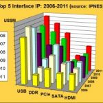
    If we look at the Interface IP business during the last 5 years, USB, PCIe and DDR were the most important, followed by HDMI and SATA. But the forecast for the 2012-2016 (see above) clearly shows that, if USB and PCIe are still part of the Top 5, DDRn and MIPI IP will see the higher growth (DDRn IP being also the largest segment). This simply means that Cadence is well positioning to fight with Synopsys in the near future, as the company being already strong in DDRn IP, present in PCIe IP, is now strong in MIPI PHY IP and present in USB PHY IP, thanks to this acquisition.

    So, I would agree with Martin Lund, Cadence’s senior vice president of R&D for SoC Realization when he says “The addition of Cosmic Circuits’ stellar technology and talent enhances Cadence’s position as a leading provider for analog/mixed-signal IP. The combination of Cadence and Cosmic Circuits will provide customers with high quality IP to accelerate getting products to market.”

    And please don’t forget it: the PHY IP support will be an important part of the winning strategy, in this IP battle between Synopsys and cadence!Eric Esteve from IPNEST


    Please Help Me Understand IBM – Common Platform Technology Forum 2013

    Please Help Me Understand IBM – Common Platform Technology Forum 2013
    by Zvi on 02-08-2013 at 11:00 pm

    “Innovations for Next Generation Scaling”

    The 2013 Forum today (Feb 5, 2013) started with a presentation by Dr. Gary Patton, VP, IBM Semiconductor Research & Development Center. Gary very clearly articulated the two irresolvable challenges the industry now faces:

    • On chip interconnect
    • Lithography

    These two challenges connect very well with our recent blog IEDM 2012 – The Pivotal Point for Monolithic 3D IC. Gary showed both the exponential increase of RC which results from the dimensional scaling of copper below 100nm width and the high cost associated with double and quad patterning. In addition, he showed how the extreme scaling of the copper metallization creates reliability challenges such as fatal EM modes, and scaling of the insulator k breeds TDDB and strength issues. As a reminder, in the recent IEDM (Dec. 2012) short course, IBM presented the following slide indicating that interconnect now dominates device power!

    L. Chang, D.J. Frank – IEDM 2012 Short Course – IBM Watson Research Center

    Gary also presented a multi-decade past to future slide that resembles the one presented here below. The decade ending at the year 2000 was the good old days of easy scaling of planar transistor, which he called the gate oxide limit. Then the industry followed with a decade of “Material Innovation” that he called the planar device limit, and starting in 2010 is the beginning of the “3D Era” – 3D transistors and stacked devices.

    Finally he shared with us his vision of 3D devices with three planes of devices:

    • Logic Plane
    • Memory Plane
    • Photonic Plane

    A vision we mutually share.

    Now, here is my failure to understand. As a company who has been in the forefront of 3D and TSV research, IBM is well aware of the severe limitations of TSV as an alternative for vertical interconnect. The following cross-sectional picture by IBM, presented at the recent GSA Summit, clearly illustrates how large a TSV is in comparison to an interconnect via.

    IBM Systems and Technology Group – GSA Silicon Summit 2012 (S.s lyer) – 2012 IBM Corporation

    With TSVs of 5 micron diameters (and pitches of 15 micron due to keep out zones from stress issues) vs. vias of less than 50 nm, the ratio in vertical connectivity is 1:10,000 as illustrated in the following chart by Perinne Batude of CEA Leti.

    Clearly IBM technologists are well aware of the many research papers showing that TSVs, with their relatively huge size compared to all the other on-chip elements, diminish the performance or power benefits in folding designs to 3D. For example, the chart below was presented by Kim at the 2011 IEEE International Interconnect Technology Conference. The chart illustrates the performance benefits of folding a design twice (4 tiers of transistors) as dependent on the via size. At a via size of 5 microns there are actually no benefits, while at a via size of 0.1 micron the benefits are the equivalent of two nodes of dimension scaling!!!

    So can someone please explain to me how come IBM is still talking about TSV as if it is the only representative of the “3D Era”???

    And particularly now, when monolithic 3D is finally practical, and the NAND Flash memory vendors are adopting it across the board!?


    Another Winner at DesignCon

    Another Winner at DesignCon
    by Daniel Payne on 02-08-2013 at 5:44 pm

    After a show like DesignConwraps up we get a chance to ask ourself what it all meant, and how was this year different than last year. Reading through many posts about DesignCon I came to discover that the Awards at DesignCon are less contentious than at CES, and also that ANSYSreceived a DesignVision awardfor the 2nd year running. Their winning tool in the category of Modeling and Simulation is called HFSS for ECAD.

    Typically the design engineer doing PCB layout would use Cadence tools, then export their design data, ask the SI expert to import them into a field solver like HFSS, setup and run the field solver, interpret the results, and communicate verbally with any recommendations. Not a very productive flow, so the process has been integrated quite a bit.

    You can now stay working in your familiar Cadence layout tools and launch HFSS for analysis:

    • Allegro PCB Designer
    • Allegro Package Designer
    • SiP Layout
    • Virtuoso Layout Suite

    The software that enables this integration is called:

    • ANSYS HFSS, or HFSS solver-only option
    • ANSYS Designer Pre-Post, or ANSYS DesignerSI
    • Ansoft Links for ECAD

    Using this combination of ECAD tools from Cadence and field solver tools from ANSYS lets engineers design and quickly analyze chip, package or boards where you need a 3-D model to take into account high-speed interconnect or complex packaging structures. The manual steps have been eliminated and the setup streamlined, so that you can stay in the Cadence tools to run field solver jobs like:

    • HFSS port drawing and setup
    • Automated clipping of nets
    • Setup of HFSS meshing frequency
    • Frequency sweep type, and range setup
    • HFSS convergence criteria
    • Solver and basis function selection
    • Airbox definition

    Summary
    If you want to save some time and agony, then consider looking at this integration between Cadence and ANSYS tools for your chip, board and packaging design challenges where a 3-D field sovler is required. I’m glad that Mark Ravenstahl of ANSYS talked with me two weeks ago about what to look for at DesignCon in 2013.