Bronco Webinar 800x100 1

Why IP Must Be Defended

Why IP Must Be Defended
by Randy Smith on 02-17-2013 at 7:00 pm

A few years ago I was having breakfast with Jim Hogan at our favorite place to meet in Los Gatos. I was CEO of Polyteda and Jim was Chairman so we always had plenty to talk about. This time, however, the talk had turned to protecting a company’s intellectual property (IP). Jim had brought up the topic in the context of the looming legal battle between Sonics and Arteris. Unfortunately, I steered the conversation back to my EDA roots and the Cadence-Avant! legal battle. I would have learned more if I had just listened. Semiconductor IP is not quite like software IP as there are different methods of protection, such as mask works, and patents may be easier to spot in circuits than in code.

Recently Tela Innovations, where Jim Hogan is on the board of directors,filed two actions against a group of companies who are in the mobile phone industry alleging that these companies had illegally used Tela’s patents in their products. I was surprised by the initial reaction of some in the EDA community remarking that Tela was suing its customers. Some sites have since edited or even removed some of their earlier comments. The simple fact is that if you are an IP company and you have evidence that some company is using your IP without proper licensing you MUST defend your IP. It is obvious in other industries where stores prosecute shoplifters, so why would IP be any different? They’re not yourcustomer if they are stealing from you.

Why do I use a strong term like “must”? Well, think about all the obligations that the company has; or, as board members and executive think of it – think of all of your stakeholders. First, you have an obligation to your investors. They put money into the company on the promise you were going to build something of unique value. For an IP company your patent portfolio represents a significant chunk of your company value and that value is partially owned by the investors. You must protect them. Secondly, you have paying customers to whom you sold a license to your IP. If you let others use it without paying for it is that fair to them? You also have your own employees to protect. If the company fails because the IP becomes free to use by anyone with the temerity to use it without paying for it then the employees may lose their jobs and the employee stock options become worth less (or worthless) as well. Even the community the company operates in will be damaged if the company is not there to continue to provide benefits to that community. For those that believe in karma, you may also feel that cosmic justice plays a role as well.

Tela’s filing with the U.S. International Trade Commission (USITC) alleges that various corporations including HTC, LG, Motorola Mobility, and Nokia have imported products which infringe seven of Tela’s patents. A similar action was also filed in federal court in Delaware. Tela can hope for a somewhat quick resolution from the USITC because that body is in place to stop trade practices before the violators gain much benefit from their actions. But, the companies Tela is bringing the actions against have a lot resources and no doubt the ability to drag this out some if they choose. Presumably, Tela is in a strong enough position to fight this battle a long time if necessary.

I cannot declare that Tela is right or that Tela will be victorious. I have not had the chance to read all of the filings and supporting evidence. The documentation is substantial so passing judgment now would be like voting on the voluminous Obama Care healthcare act without actually reading it. Hmmm… well, uh, anyway my heart tells me that Tela certainly believes it is correct in taking this action. Besides my longtime relationship with Jim Hogan, I believe in the character of others at Tela (Scott Becker, Drumil Ghandi, etc.) whom I worked very closely with at Artisan Components.

I have a background in semiconductor IP having worked at TriMedia Technologies and Silicon Architects in addition to working at Artisan Components. I also was a co-founder of Tangent Systems, which is where part of the code stolen by Avant! from Cadence originated. I am sensitive to protecting a company’s IP. If Tela’s allegations are indeed accurate the whole of the IP industry, and probably the EDA industry as well, needs to have Tela prevail, and sooner rather than later. Otherwise, many more alleged thefts will occur.

ISSCC 2013: Circuit Design Using FinFETs!

ISSCC 2013: Circuit Design Using FinFETs!
by Daniel Nenni on 02-16-2013 at 8:00 pm


One of the privilages of blogging for SemiWiki is invitations to the top conferences around the world including the International Solid-State Circuits Conference (ISSCC) in San Francisco this week. Amazing, this conference is older than I am:

ISSCC 2013 is the 60th Conference in an incredibly long-lasting series. Following the invention of the transistor in 1947, there was a developing interest in transistor circuit design. This coalesced in 1954, with the creation of the first “Conference on Transistor Circuits”, held in Philadelphia, sponsored by the IRE, one of the predecessors of the IEEE. Since then, transistor-circuit design which evolved into integrated-circuit design has changed the world like no other technology ever has. Propelled by this sixty-year history, ISSCC 2013 will provide a special opportunity for looking back to the future, toward further exciting developments in solid-state circuits and systems. ISSCC remains the premier forum in the world where circuit innovations are presented. In this role, ISSCC will continue to (em)power the future!

The advanced program is HERE, if you want to avoid me do NOT attend these sessions:

T4: Circuit Design using FinFETs
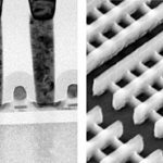
After HKMG, FinFETs are a powerful yet disruptive technology to enable continuous scalingfollowing Moore’s law. The disruptive nature arises from both the 3D structure and the quantization on width choice. FinFETs require new design skills to trade-off among PPA (powerperformance-area) and to conduct circuit-process co-optimization. Salient advantages ofFinFETs include: increased driving capability per footprint area, better control on short-channeleffect, subthreshold slope, and less requirement on channel doping. Thus, threshold voltagecan be reduced, which enables a reduction in supply voltage and thus power consumption or increase of performance speed.

The tutorial will focus on critical issues of FinFET design: It starts with a crisp comparison ofplanar vs. 3D FinFET devices and the associated SPICE modeling. Next, logic design is presented,including effects on standard cells, I/O circuitry, and ESD. Then, the subjects of SRAMand analog/mixed-signal design are treated in detail. Digital chip-level design that requiresmethodology enhancement and new CAD tool features are carefully discussed. The tutorialwill enable CMOS designers to systematically comprehend circuit design using FinFETs.

As I have mentioned before, FinFETs will be the most significant piece of technology we, as semiconductor ecosystem people, will experience this decade. Attend every FinFET seminar, read every FinFET paper, stay glued to SemiWiki because FinFETS will set the semiconductor ecosystem on fire. FinFETs will keep the mobile world powered up, FinFETs will set the foundries apart. It’s coming, believe it.

ES3: High-Speed Communications on 4 Wheels: What’s in your Next Car?
Communications inside vehicles is experiencing a growing demand due to applications likeinfotainment, driver assistance, safety systems and diagnostics, requiring data-rates beyondwhat is offered by current solutions.

Considering that cabling is the third highest cost factor and the third heaviest component inthe car, there is a clear need to go beyond the current low data-rate solutions and convergeto a high data-rate backbone network. Solutions, both electrical and optical, are being proposed by car-makers and silicon manufacturers. The evening session will give an overviewon the status and outlook on an emerging market that is already shipping 650 million communication ports per year.

One of the biggest disappointments at CES this year was the cars of the “future”, we can do better.

EP3: Empowering the Killer SoC Applications of 2020

A distinguished panel from global industry and academia will debate the nature of systemsdriving the killer applications of 2020. Can we forecast the future killer applications? We havehad the computing revolution, then communications, and now the sensor era. Are sensorsdriving the next killer applications? Are there any other revolutions in sight? What circuitsand system innovations can ISSCC bring forward for the next killer applications? What technology elements, device structures and memory architectures are required? Should we continue with silicon technology and find breakthroughs through system architecture, algorithms, SoC integration and packaging? Or should we prepare for “beyond silicon” technologies? Are any beyond-silicon technologies realistic for the future?

For those of you who don’t know, Fisherman’s Wharf has great seafood and is a Cable car ride away. Scoma’s is my favorite but just eating a bowl of cioppino on the waterfront is fine too. The weather looks good but bring an umbrella because it is San Francisco and you just never know. I have an ISSCC umbrella from last year somewhere.


Aldec Delivers Leading Verification Methodologies!

Aldec Delivers Leading Verification Methodologies!
by Daniel Nenni on 02-14-2013 at 8:15 pm

For those of you who don’t know, Aldec Inc., headquartered in Henderson, Nevada, is an industry leader in Electronic Design Verification and offers a patented technology suite including: RTL Design, RTL Simulators, Hardware-Assisted Verification, ASIC Prototyping, Design Rule Checking, IP Cores, DO-254 Functional Verification and Military/Aerospace solutions.

I first met Aldec at DAC and was very impressed by the focus they have on training and education. You can find a nice list of white papers HERE, multimedia webinars, videos, and demonstrations HERE, application notes HERE, and tutorials HERE. And of course the Aldec SemiWiki landing page is HERE with coverage by Daniel Payne and Don Dingee.

Aldec has an important DO-254 Training Event (Webinar)coming up that we are all invited to:

DO-254 Verification Strategies

Date:Thursday, February 21, 2013
Time:11:00 AM – 12:00 PM PST
Presenters:
Louie DeLuna – Aldec DO-254 Program Manager
Daniel Conway – X-Tek DO-254 Consultant

Abstract:
As a best-practice standard, efficient ASIC and FPGA project planners will allocate 1/3 of the project cycle to design and 2/3 of the project cycle to verification. The best of these planners will bias toward even more verification-hours and innovative verification strategies whenever possible, because the great reality of schedule-time allocated to verification is that THERE’S NEVER ENOUGH TIME.

When an FPGA or ASIC is destined for an avionics product, effective design of that DO-254-qualified device is even more dependent-upon good verification strategies and practices. Good verification strategies will use those precious hours more effectively – and will also consistently prove to be more useful when combined with a comprehensive exploitation of well-written requirements and compliance with a well-constructed verification process, planned in advance of the work.

REGISTER HERE

In this webinar, we will discuss various verification strategies and how they can be applied to successful verification of a design in a DO-254 Levels A/B flow.

Agenda:

  • How and where verification fits into the overall process
  • Verification Strategies
  • Ad-hoc testing
  • Directed testing
  • Constrained random testing
  • Verification Architectures
  • Driver – Waveform
  • Auto-checking
  • OVM/UVM
  • Code coverage and its proper usage
  • Documentation and reviews
  • Test plan vs. test cases
  • How to pass the audit
  • Q & A

Aldec is a proven EDA solutions provider delivering leading verification methodologies that support the latest language standards enabling their customers to grow while leveraging evolving technologies. Definitely worth a look, their corporate website is HERE.

RTCA/DO-254 and EUROCAE/ED-80 are means of compliance for the development of airborne electronic hardware containing FPGAs, PLDs and ASICs. FPGA design and verification under DO-254 guidelines is a rigorous undertaking, and requires special features and capabilities from design, simulation and hardware verification tools.


Patenting in the (Resistive Memory) Material World

Patenting in the (Resistive Memory) Material World
by Christie Marrian on 02-14-2013 at 8:10 pm

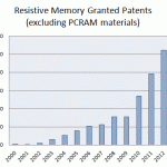
(with apologies to George Harrison) Two recent Blogs over at ReRAM-Forum.com have focused on the latest in the IP field, particularly as it affects resistive memory. A high level overview of who is patenting what suggests a healthy amount of R&D is going on in the field. But looking a little deeper suggests there is much overlap amongst some supposedly key patents. Perhaps this is inevitable for an emerging technology but people familiar with the field point out that this in fact an impediment to the introduction of the new technology. On the other hand, the belated arrival of PCRAM suggests this can be overcome, at least during the early stages of a product gaining traction in the market place. Unfortunately, these days, it is a sign that a technology has gained a foothold in the market when the lawsuits start flying!

Alerted by Beth Martin’s Blog here at SemiWiki, we’ve also looked at the impact of the HR. 1249 aka America Invents Act (Image shows President Obama signing the act into law along withand the Sponsors andstudents of Thomas Jefferson High School, Alexandria, VA). Under the Act, the US is changing from a First to Invent system to a First to File (actually First Inventor to File possibly for reasons of constitutionality). This legislation was heavily sponsored and lobbied for by the Tech Lobby and all sorts speculation has ensued that this is a plot to stifle the small entrepreneur. I’m not totally convinced and there are upsides to the Act such as (the promise of) a faster (1 year) examination timeline, filing fee discounts for the new class of ‘micro entities’ (individuals and universities) and revised post grant procedures. Nonetheless, I’m sure the litigation lawyers won’t be going out of business anytime soon.

Interestingly a couple of resistive memory related job openings have appeared recently; one on each side of the pond. While not as big of a story as the famous ReRAM job position advertised by SanDisk last year, it good to know that people are still hiring.

On the technical side, we are taking a look at IBM’s MIEC BEOL access device for ReRAM/CBRAM and PCRAM. This almost seems to be the ‘perfect’ diode with an enormous on/off current ratio. IBM has been quite open with performance and processing data although the composition of the material stack is not made clear. Which takes me back to searching through Patents and Patent Applications!

Christie Marrian, ReRAM-Forum Moderator and Real (Court) Tennis player


Functional Check List in Verification

Functional Check List in Verification
by guruvadhiraj on 02-13-2013 at 8:25 pm

This article tries to bring out the advantages of having a functional check list. The objective is to make verification as robust as possible. Functional check list ensures the complete coverage of hardware block that is designed. This may to an extent help software developers. Creation of test plan with functional check list as the base will result in creating a test plan which covers end to end of hardware block. Functional check list might already be existing in some of verification process as on today but some sections audience might have missed out.

First lets describe the role of having a check list of functionality that hardware block is designed to perform. The intention of this step is to make sure that none of the functionality of hardware block is missed and the coverage of various scenarios. Secondly, of late I have seen some influence of software requirements having some impact on verification. Let us take an example of uart, if the hardware engineer is having an input that software engineer will use ‘x’ baud rate, then there is possibility that that hardware engineer will make sure that ‘x’ baud rate works perfectly fine and few baud rates around that baud rate. For other baud rates, he may or may not do the verification which could be because of two reasons

[LIST=1]

  • Time constraint
  • Necessity

    If the reason was former then it is understandable though it is not convincing. If the reason is later then it is advisable to change the perception.

    Functional check list helps in identifying the test case/scenario’s that was missed during verification. In the above case of UART , if the verification engineer misses some of the baud rates then comparing the result of verification to functional check list will bring out the missed scenarios.

    It also helps in identifying the corner cases, random and regression testing before proceeding with the verification/test plan.
    Typically Asic Design has the following steps

    [LIST=1]

  • MRD
  • Architecture specification
  • Design Specification
  • Verification Plan
  • RTL Design
  • Functional verification
  • Synthesis
  • Physical Design
  • Timing Analysis
  • Tapeout

    Functional check list falls between step3 and step4, i.e. when design specification is ready , functional check list is created.

    [LIST=1]

  • MRD
  • Architecture specification
  • Design Specification
  • Functional Check list
  • Verification Plan

    Let us see some simple implementation by having counter as an example. Assume that this counter can perform incrementing count and decrementing count, Interrupt signal when count matches compare value, different clocks and Auto Reload.


    Functional check list

    [LIST=1]

  • Increment count with basic/default clock rate
  • Different Compare value(actual values can be written) and interrupt generation
  • Different clock rates of a,b,x,y,z
  • Auto reload with different values
  • Decrement count with basic/default clock rate
  • Different Compare value and interrupt generation for down counter
  • Different clock rates of a,z for decrement count
  • Auto reload with different values
  • Interrupt disable

    Above list describes the functionality of the counter. we can find that some of them in the above list is repetitive for e.x : different clock test when counting up and counting down. This is to ensure that hardware block is tested in all scenarios as much as possible.
    There can be two more list called as negative list where negative scenario’s can be mentioned and regression list. Negative and regression list is not mentioned here as there is not much for the counter module.

    Before starting the verification we can have

    [LIST=1]

  • Functionality list
  • Negative list
  • Regression list

    As the complexity of hardware increases so is the checklist. When there are signals interfaced to the hardware block, it can be written along with one of the functional list. As explained in counter there is interrupt signal when counter matches compare value. Therefore this can be further written as two columns.

    [TABLE] border=”1″
    |-
    | style=”width: 319px” | Functional list
    | style=”width: 319px” | Signal name
    |-
    | style=”width: 319px” | Different Compare value and interrupt generation
    | style=”width: 319px” | INT0 (Interrupt signal name)
    |-

    Table 1

    This list helps the verification engineer in writing the test plan and test bench. This gives overview of verification engineer’s understanding of the hardware block. When the hardware complexity increases , time spent on this activity would be more but significantly reduces the effort in feature extraction. With this kind of approach Integration of blocks becomes much easier.


    Let us take another example which does the generation of signals. In this example Consider Block X having 3 registers as reg_a, reg_b, reg_c. The functionality of this block is to generate signals based on programming the registers. This block may not have much functionality like the counter but signal generation is the main task of this block. In such cases we can the functionality list as mentioned below

    [TABLE] border=”1″
    |-
    | style=”width: 296px” | Functional list
    | style=”width: 295px” | Signal to be asserted
    |-
    | style=”width: 296px” | Reg_a =1
    Reg_a =0
    | style=”width: 295px” | X_a =1
    X_a =0
    |-
    | style=”width: 296px” | Reg_b =1
    Reg_b =0
    | style=”width: 295px” | X_b =1
    X_b =0
    |-
    | style=”width: 296px” | Reg_c =1
    Reg_c =0
    | style=”width: 295px” | X_c =1
    X_c =0
    |-
    | style=”width: 296px” |
    | style=”width: 295px” |
    |-
    | style=”width: 296px” | Different clocks x,y,z
    Reg_a =1
    Reg_b =1
    Reg_c =1
    | style=”width: 295px” | X_a =1
    X_b =1
    X_c =1
    |-
    | style=”width: 296px” |
    | style=”width: 295px” | X_a =0
    X_b =0
    X_c =0
    |-

    Table 2

    Looking at the above table, second column gives the opinion of expected result. The answer is yes . For models such as the one mentioned above signal generation is the main functionality.

    These are basic examples that are discussed. There are many hardware blocks with complex systems and complex interfaces. The above table becomes complex with the complexity of the module/chip.

    The next question that would arise is why not expected result as one of the columns in counter block?

    Expected results can be included in test plan where as the functional check list concentrates on functionality coverage
    To put it in simple words, with the functional check list chances of missing the corner cases is less
    Is functional list different from Feature Extraction?

    Objective of the functional list and Feature Extraction is same. In this case, feature extraction can be considered as subset of functional list.

    Functional check list will help in systematic approach to verification. It will help in identifying the test bench requirements and approach to functional verification. It is up to verification Engineer to decide the usefulness of this approach.

    This is a suggestion. Comments and feedback are welcome. I can be reached at LINKEDIN :
    in.linkedin.com/pub/guruprasad-pv/9/947/9b1

    guruvadhiraj@gmail.com/gurushesha@gmail.com


  • Developing ARM v8 Code…Today

    Developing ARM v8 Code…Today
    by Paul McLellan on 02-13-2013 at 12:50 pm

    You are going to be developing software for an SoC that contains an ARM Cortex-A57 64-bit CPU. Or perhaps it is an SoC containing ARM’s hybrid big.LITTLE multi-core architecture that combines one or more low power cores with some high power, high performance cores to get the best of both worlds: high throughput when it is needed and low power when it is not.

    The old way of doing things would be to wait for reference boards that at least contained the processor. As a Japanese engineering manager memorably told me when I asked him what they did during that waiting period, they “pretend to program.” But these days even waiting probably won’t work. No silicon implementation of the processor is likely to be available until the SoC tapes out, and a lot of the software is already meant to be ready by then.

    A solution to this quandary is to use a Virtualizer Development Kit (VDK). This allows you to put together a virtual platform containing the core and key peripherals and start doing software development. And not just of the “pretend to program” type. You can actually run the binary code, set breakpoints, and debug in all the usual ways you would normally expect. In fact, since there is more visibility into what is going on inside the core, more ways that you would normally expect.

    The Synopsys VDK comes with full support for Linux, Android and, for the big.LITTLE cores, task migration software. Of course an complex multi-core big.LITTLE architecture combining either ARM v7 cores (Cortex-A15/A7) or v8 cores (Cortex-A57/53) requires good analysis capabilities to optimize performance versus energy. The VDK is also integrated with debuggers from ARM themselves, from Lauterbach and from GNU. The basic idea is that all the software development can be done before the SoC is available. Moreover, for multicore designs that are inherently non-deterministic, with better control and observability and repeatability.


    The VDK also contains models for the most popular DesignWare interface IP, along with device drivers and middleware. So if your SoC contains USB 3.0, USB 2.0, Ethernet GMAC, mobile storage and I2C then it is straightforward to configure a virtual platform and the operating system appropriately.


    Of course ARM’s portfolio of cores isn’t static and new cores will appear in the future. Synopsys and ARM have signed a long-term collaboration agreement for VDKs going forward, ensuring that investment in development environments can be leveraged as new cores are announced.

    More information on Synopsys’s VDKs is here. The full datasheet (registration required) is here. More information on the specific challenges of integrating DesignWare interface IP is here. The press release about the collaboration agreement with ARM is here.


    Welcome to the Video Club!

    Welcome to the Video Club!
    by Eric Esteve on 02-13-2013 at 12:26 pm

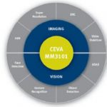
    CEVA is happy to welcome new competitor in the DSP IP solution for Computer Vision and Imaging elitist club! In fact, we all know that the competition is not only good for IP customers, but is also a good way to boost innovation and propose continuously improved solutions, and Computer Vision and Imaging is one field of high creativity, in the Mobile and MultiMedia applications. To be frank, CEVA was feeling lonely since the company has first offered the MM3000 DSP IP solution for Imaging, back in 2010. They have launched the third generation, MM3101, offering multiple enhancements like Power Scaling Unit (PSU) or Integrated AXI, allowing to build best-in-class solution in term of power consumption and TTM through easier integration, both being key differentiators in the Mobile industry.

    As Paul McLelan has explained in a brilliant post, processing the algorithms for Image Enhancement, like Video Stabilizer, Local DRC, HDR or Super Resolution, and Computer Vision, like Face Recognition, Gesture Recognition, Gaze Detection or Forward Collision Warning, is simply not possible anymore on ARM CPU core or even GPU core: the associated power consumption is far too high, in the multiple Watt range, when the allowed power budget is in the mW range! Clearly, DSPs as a more viable option than offloading imaging and vision tasks to a GPU, which has proven challenges with regard to performance, memory bandwidth, die size and especially power. We know that the new paradigm in the SC industry is power consumption rather than pure performance.

    Or I should say, as low power budget as possible to run a specific task, which could demand very high performance level. Let’s take the example of a 32-bit integral image computation on 16b pixel data at 1080p30: the power consumption would be one Watt with ARM core, a few hundreds mW with a GPU core, evaluated to be 10.8 mW by one of our competitor… and less than 3 mW for CEVA MM3101 (at the same conditions: 28nm HPM process, regular Vt). The secret sauce here is: Experience and Architecture. CEVA has built the 3[SUP]rd[/SUP] generation of DSP IP core based on a flexible architecture (see picture). VLIW and SIMD is not enough, the core must be able to be flexible in the operation and not rigid in terms of units doing same operation and capability operating enough units in parallel.

    But low power does not mean poor efficiency. Let’s take another benchmark, a normalized cross-correlation function on 16-bit pixel data with 32-bit accuracy. When competition is claiming to achieves 1 million 8×8 blocks per second, CEVA has demonstrated one order of magnitude better performance, with 12 Million blocks per second!

    Once again, there is a secret sauce here. CEVA integrates a Power Scaling Unit (PSU), able to provide as much power as needed during computation, and drastically reduce power after. Such a technique could be implemented by SoC designer, but would take time, so, when CEVA provide it in their solution, it’s better for TTM! As well, CEVA standard solution for Imaging integrates AXI Bus, as well as Memory and Control cache management, so the SoC designer just need to select and integrates the memory… Once again, shorter design cycle allows better TTM!

    CEVA will show several demos, built by their customers, like Gesture Recognition and Tracking, Face Recognition, or Lane Departure Warning (LDW) for Advanced Driver Assistance Systems (ADAS) applications, to name only a few. This also means that CEVA DSP IP Imaging solution is Silicon proven. But if you need a development board to build your own demonstrator, it’s available from CEVA, as you can see on the picture below.

    Just to finish, let’s mention that CEVA solutions for Imaging and Computer Vision are implemented in multiple application, starting with Mobile, which is probably the largest market, up to MultiMedia or Surveillance.

    Eric Esteve from IPNEST


    SoC Implementation, Sometimes You Need a Plan B

    SoC Implementation, Sometimes You Need a Plan B
    by Daniel Payne on 02-13-2013 at 11:14 am

    I read two blogs this week that got me to thinking about contingencies in SoC implementation. By contingency I mean using an EDA tool flow from the leading vendor for logic synthesis and then discovering that you cannot route the design without expanding the die size after a few weeks of concerted effort, then having to come up with a Plan B. The blogs were from two people at Oasys Design Systems:

    This AE named Ganesh Venkataramani talks about visiting a semi company in the mobile market that had a chip in tape-out that was growing too large because of congestion. They couldn’t even fit the whole chip into their logic synthesis tool at one time, so that made it tough to figure out if there were any top-level timing issues.

    Large SoC design teams have separate front-end and back-end engineers that perform very different tasks with different logical and physical IC design tools. This particular design team decided to give Oasys tools a shot on resolving their routing congestion dilema, I mean what did they have to lose?

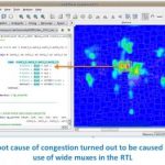
    With the help of the AE they were able to get their design loaded into Oasys tools in a day. The physical synthesis tool is called RealTime Explorer, and it could synthesize the entire SoC in a couple of hours. Next, they visualized the results by cross-probing between the routed IC layout and RTL source code to identify the source of congestion. Plan B worked out quite well for this design team because now they had pin-pointed their routing congestion back to the RTL where wide muxes had been used. Pretty impressive for just one day’s work compared to previous efforts that fell short after weeks with multiple engineers.

    The second blog was written by Dan Ganousis, an EDA veteran who started out as a design engineer just one year prior to me back in the 1970’s. His blog also focuses on the implementation issue of routing congestion.

    So what happens when the front-end RTL team assembles all their IP, writes new code, verifies the logic, does some logic synthesis, then throws the design over the wall to the back-end IC implementation team? Often the result is an IC design deemed “Unroutable”. The good news is that using an EDA tool like RealTime Explorer can let you cross-probe between the physical and logical worlds:

    The screenshot above shows the physical routing congestion on the right, where Red is the area of highest routing congestion. The cross-probing lets you quickly identify the RTL source code responsible for causing this congestion, so now you know what to modify in RTL to improve your physical layout.

    Here’s the big picture view of analysis features that you’ll find in RealTime Explorer:

    Summary
    If your present EDA tool flow isn’t creating the chip size that you want, or getting out of tape-out quickly enough, then consider calling Ganesh as your Plan B.


    An Affordable AMS Tool Flow gets Integrated

    An Affordable AMS Tool Flow gets Integrated
    by Daniel Payne on 02-13-2013 at 11:10 am

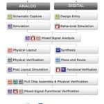
    EDA tools come in all sizes and price ranges, so I was pleased to readthat Tanner EDAhas completed an integration with Incentia. A few months ago Tanner announced their integration with Aldec for digital simulation, and today’s announcement extends their tool suite to include digital synthesis and static timing. Here’s the entire integrated AMS tool flow:

    Continue reading “An Affordable AMS Tool Flow gets Integrated”


    Extending Wintel collaboration to Nokia?

    Extending Wintel collaboration to Nokia?
    by gauravjalan on 02-12-2013 at 10:00 pm

    Any article or blog on mobile phones talks about the ongoing battle between Apple and Samsung or the never ending struggle of Nokia and Blackberry. These reports are primarily based on the US market that hosts close to 322 million mobile subscriptions as per report in DEC 2012 by mobiThinking. With 81% (256 million) of the US population on 3G/4G i.e. Smart phones, it makes sense to have the articles talk around them. While the US leads the market in terms of product launch and adoption, 30 percent of the world’s mobile users live in India and China. China leads in terms of subscriptions with 1+ billion subscribers out of which 212 million are 3G/4G users. India is ranked second with 906.6 million total (699 million active) subscribers and only 70.6 million 3G/4G users. This means it will take quite some time for the Smart phones to overtake feature phones and the reasoning might be dropping price point and not the need from consumer unless a killer application cuts in. What it also means is that with Nokia still leading the feature phone market, it has some room left to pick up.

    This belief of mine turned stronger when I visited a few stores in search of a phone recently. My wife’s touch screen CDMA phone from a leading brand lost its touch sensitivity again. It has already demanded service twice in last 5 months. Infact, it was the 3[SUP]rd[/SUP] CDMA phone bought in 2 years while our GSM one still continues to operate smoothly. With limited CDMA phone options available it was always a compromise on the handset. The reason for sticking to CDMA was the unlimited talk time plan offered by one of the carriers. With the capital cost balancing the savings on operating cost, we decided to transition from CDMA to GSM that has full range of handsets. With a tablet available for internet browsing, the usage of phone is limited to calls. Taking a rational approach, we decided to look for sub $200 phone to overcome this need (still guessing if the result was an outcome of my convincing capability or my wife’s ability to understand the logic). Note – In terms of carriers providing the handsets with a 1 or 2 years plan, India has limited options. The phones are bought mostly bought directly from stores hosting a range of handsets from a variety of sources.

    On our visit to the store, there was a wide range of options within $200 price tag and Nokia was clearly leading the range. The price points for the features offered were amazing. Samsung failed to impress in this category and there was not a single handset from LG. While there were a lot of Chinese phones but the packaging is still poor and no matter if they provide double the features for the same price, if the phone hangs, God help! For a $200 phone category, one of the impressive sets was Xolo from Lava powered by Intel Atom. It had the largest display with clarity and maximum features in this price category. Finally Nokia won the choice by being closest to the requirement in all respect.

    After reaching back, I checked on the latest reports on the Indian market to validate our buy. According to CMR’s India Mobile Handsets Market Review, 2Q 2012, September 2012 release, during 1H 2012 (January-June 2012), total India shipments of mobile handsets was recorded at 102.43 million units. During the same period, total India shipments of smart phones were 5.50 million units. Interestingly Nokia still leads the market here.

    Even in the Smart phone market in India, Nokia still has a strong presence followed by RIM. No Apple yet!

    The cell phone market in India is unconventional in terms of handsets, services and usage but carries strong potential. Considering the developments in this domain, what if Nokia enters the Wintel partnership directing it to the cell phone market? Intel recently announced that it is looking to attack the lower price segment to increase foot print in the mobile segment. Nokia already has tied up with Microsoft for its OS. Why not extend this partnership further and make a ‘NokWinTel’ or ‘WinTelKia’. The later could be interesting as “Kia” in Hindi means “did” giving the partnership a regional flavourJ. All 3 are recognized as top brands in the local market. They need to hit the right price points with a variety of products along with look & feel. If this trio (Microsoft, Intel & Nokia) is able to collaborate and attack this LONG FAT TAIL, all 3 would be able to claim a bigger share for their respective products.