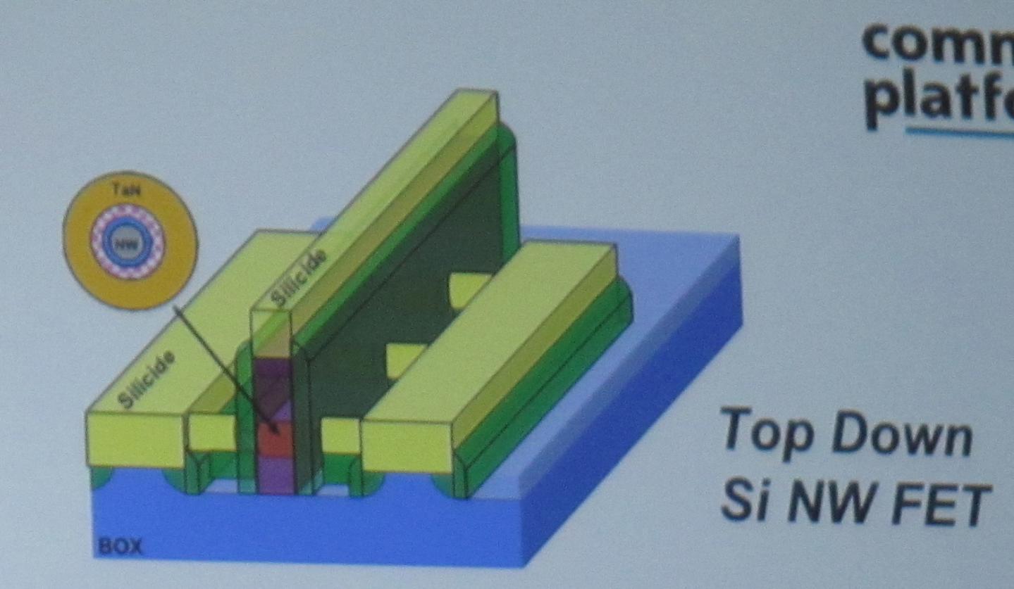


 So what is a silicon nanowire? It is basically a FET where the active element is a wire 3-20nm in diameter. So where a FinFET has the gate wrapped around 3 sides of the transistor, a nanowire (NW) has it wrapped around all four. In essence, the wire runs through the middle of the gate.
There seem to be three issues about building a silicon nanowire. First, suspending the wire above the substrate, then depositing the gate around the wire, and controlling the shape of the wire (you’d like it to be as circular as possible). One thing you can do with NW that is new is to run several wires through the same gate, either to switch multiple signals simultaneously or to get higher current.
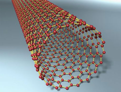 Beyond 7nm, silicon is not the ideal substance for nanowires and it is better to use carbon nanotubes. A carbon nanotube FET (CNTFET) has much higher currents compared to silicon. This has the potential of an enormous increase of 3-10X in power and/or performance. Carbon nanotubes are a roll of carbon 1nm in diameter. The bandgap can be adjusted which means we can have both normally-on and normally-off transistors (like “p” and “n” type transistors in CMOS) and so we can continue to use complementary logic.
The fabrication process is completely different than for silicon NW. The carbon nanotubes are created as a sort of raw material away from the wafer fab. One issue is that some percentage of them are metallic rather than semiconducting and so repeated purification steps via column chromatography are required to ensure that (almost) none of the metallic ones get through.
The carbon nanotubes are then laid onto the wafer in a single layer at 6nm spacing. Using cut masks these can then be patterned.
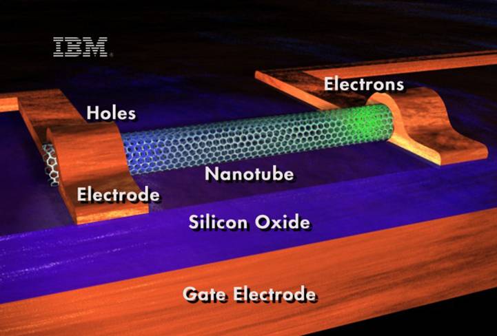
One big challenge to be solved with CNT is that currently we don’t have a good way to contact to them without requiring an extremely long (say 300nm) contact area. This will need a lot of work to solve to make CNT practical.


Consolidation and Competition: Who is Winning the $4.5 Billion Interface IP Race?