webinar IPXACT banner

Thermal Reliability and Power Integrity for IC Design

Thermal Reliability and Power Integrity for IC Design
by Daniel Payne on 09-14-2015 at 12:00 pm

When I designed DRAM chips at Intel back in the 1970’s we didn’t really know what the die temperature would be before taping out silicon, instead we waited for packaged parts to come back and then did our thermal measurements. IC designers today don’t have that luxury of taping out their new SoC without having done some simulations for thermal reliability and power integrity. As an IC is powered up the active transistors start to warm up the local area of the chip, which in turn slows down the timing and reduces the current drive capabilities, so this interdependence needs to be simulated. From a reliability viewpoint the current through the interconnect creates a voltage drop (aka IR drop) and the integrity of the metal interconnect depends on how many amps per square micron that can flow before electromigration effects set in (EM).

I’ve blogged about an EDA vendor named Invarian back in 2013 at DAC when I first learned about their power, thermal, EM and IR tools, then Silvaco acquired Invarian in March 2015. Alex Samoylov from Silvaco spoke with me by phone recently to provide an update on their tools in this area.

Q&A

Q: How do your power integrity tools fit into the design flow?

They can be used for standard cell designs at the gate-level, SoC or full-chip level, even at the transistor-level for analog and custom designs.
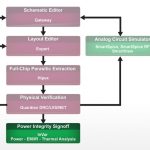

InVar Design Flow

Q: Is InVar three separate tools?

No, InVar is a bit different than other approaches because it’s a single tool with three types of analysis: Power, EM/IR and Thermal.

Q: Who on the design team would use InVar then?

A layout engineer could start using InVar to help in the routing and planning of the power nets, VDD and VSS. InVar IR will provide them early analysis on how good the power routing is at that point.

On a standard cell approach the design engineer could start with a Verilog netlist and start running power analysis.

Thermal analysis can be run whenever you have power number for the cells.

Q: How accurate are the results of the InVar tool?

Foundries like TSMC have certified gate-level InVar EM/IR for use in their flow for 16 nm FinFET Plus (16FF+) version 1.0, so it’s a sign-off quality tool. Running power analysis on a standard cell design you will see results within 1.5% of reference numbers.

Q: How does InVar work with a SPICE circuit simulator?

If you have a transistor-level design then we use SmartSPICE as the simulation engine to produce the power analysis numbers. Typically getting pure SPICE level accuracy for power integrity analysis is a challenging task. The number of measurements and capacity requirements can quickly overwhelm the interface. Tight API level integration enabled us to deliver the capacity and speed needed to make block level EM/IR using a designers existing SPICE netlist and GDSII a reality.


Q: What kind of results come out of your analysis tools?

For EM analysis we report any violations, and then it’s up to you for fixing the violations by using a layout editor, we do highlight the interconnect segments for quick identification. Then you would rerun analysis after making your layout fixes.

Our tool provides several reports and it even has an API so that you can see a very low-level annotation of the results at Cells, pins, ports, nets or net segments.

Q: How long does analysis take to run?

In layout mode InVar is capable of completing IR drop analysis for an average design block within several minutes. InVar runs on a single host using multiple threads, producing almost linear results depending on the number of CPUs. We’ve even used up to 64 cores on designs with millions of instances.

Q: What is the learning curve like for InVar?

It’s a simple tool to learn and run, using standard format input files. We include demo scripts in Tcl with something like 50 lines of code to help automate the process for you, and there’s a demo design for learning. You can learn how to do IR drop analysis quite quickly.

Q: When should I be concerned about power, EM/IR and thermal issues for my IC design?

Probably starting at the 28 nm node and lower process geometries for digital designs, and of course for FinFET designs because current density effects reliability, the DFM rules are very complex. Even at the 180 nm node is you are doing high current designs in LDMOS then EM rules and thermal issues need to be analyzed.

Q: Why should I consider using InVar in my IC design flow?

Our tool is very easy to use, has proven accuracy of results, provides fast analysis run times, and has an affordable price. You can check out an introduction video:


We are also going to be at TSMC OIP on September 17, and I will be available at the show all day in Booth 414. I will also present an InVar webinar before the end of September and those interested will be able to register from the Silvaco web site.

Related – Analysis of Power, Thermal, EM, IR at DAC

Related – Silvaco Swallows Invarian


Replacing the British Museum Algorithm

Replacing the British Museum Algorithm
by Paul McLellan on 09-14-2015 at 7:00 am

In principle, one way to address variation is to do simulations at lots of PVT corners. In practice, most of this simulation is wasted since it adds no new information, and even so, important corners will get missed. This is what Sifuei Ku of Microsemi calls the British Museum Algorithm. You walk everywhere. And if you don’t walk to the right place, you miss something. We’ve probably all had that sort of experience in large museums like the Met or Le Louvre.

At DAC, Solidio organized a panel session Winning the Custom IC Race with participants from Microsemi, Applied Micro Circuits and Cypress (along with Solido themselves). The session was videoed and the videos and their transcripts are now available.

The session kicked off with Amit Gupta, the CEO of Solido, showing the results of a blind survey that they had commissioned earlier in the year. You can look at the transcript for the full results but here are a few of the highlights:

  • 60% of companies use 2 or more SPICE simulation vendors, only 40% use just one
  • ¼ of respondents were planning on evaluating or adding a new simulator in the next year
  • the most important features of a simulator (in order) were accuracy, foundry models, speed, capacity. Not really a big surprise. Nobody wants inaccurate results really fast.
  • 73% use Cadence, 52% use Synopsys, 33% use Mentor and there is another 25% for other simulators such as Agilent and Silvaco (of course these add up to more than 100% because most people use 2 or more)
  • the top drivers for variation aware tools were to reduce overdesign (43%), avoid respins (42%), reduce underdesign (39%), and some other factors at much lower percentages
  • when it came to actually using or planning to use variation-aware tools the percentages were 28% already using, 9% planning to, 29% planning to evaluate and 34% with no plans
  • the big requirements for such a tool were SPICE simulation reduction (50%), accuracy (49%), integration (41%) and some other much lower factors

It only gets worse with more and more advanced process nodes. As Amit said to wrap up:In addition to ultra-low power design where the amount of margin goes down and therefore the amount of variability goes up – we’re also seeing moving to smaller nodes variation becoming more of an issue, 16 nanometer FinFET transistor design or even we’re starting to see FD-SOI transistor design and at 10 nanometer multi-patterning and spacer effects.

First up of the customers was Sifuei Ku of Microsemi in the SoC division (the old Actel) who had needed an alternative to the British Museum Algorithm mentioned above, in the middle of a project. Since they are designing FPGAs they are pushing transistors to the limit and often designing beyond the well-categorized regions.

Microsemi wanted to supplement their traditional PVT and Monte Carlo (MC) with high-sigma MC. When Sifuei was asked how this compared to their previous software he had to admit that they didn’t have any previous solution. So they evaluated the possibilities. Obviously the first criteria (criterium?) was that the software needed to be able to detect issues. But since they were adopting this in the middle of the execution phase for 28nm arrays they needed it to be easy for the CAD people to set up and for the designers to use.

When they evaluated Solido’s variation designer they found some problems. Real problems.During the eval cycle it did catch several issues. We had a chip that came back, it was last year, and we did have an issue in the pulse generator in the nonvolatile memory section; the designer after a while had figured out what the problem was. However, we did the evaluation and we sent the exact circuit to Solido and their software caught it right away. So it actually zeroed into the issue that we believed the problem was. And if I remember correctly, we engaged the evaluation on Thursday, the CAD people got it up and running on Friday. The designer actually played with it on the weekend and actually on the designer’s first design, a level shifter, he found the issues on the weekend.

They also got good results with the high-sigma MC. They could never run something like this before because it would have taken literally billions of simulations which is obviously intractable. But with Solido most circuits actually converged between 500 and 1000 simulations, which is actually better than Solido’s own number where they say it will converge in 3-4000 simulations.

More recently they have evaulated Hierarchical Monte Carlo and ended up buying the tools after 2 weeks of evaluations. They did the evaluation on the full memory arrays.Solido was able to construct this memory – this 15.6 million cell array – with all the bit lines and sense amps. And actually, what we do is that we run the Monte Carlo for our chip to 3 sigma, the sense amp is to 5.1 sigma and the bit cells to 6.2 sigma.

Bottom line: they improved the design 17-55% with a saving of 1.7M times in simulation time (from a theoretical 18B to 8,000 simulations). Unfortunately they were outside their budget cycle so they had to beg for more money from their VP, but they ended up getting it so the story has a happy ending.

More from the session in another blog. The videos and transcripts for the whole session are here.


FDSOI As a Multi-Node Platform

FDSOI As a Multi-Node Platform
by khaki on 09-13-2015 at 12:00 pm

One of the main criticisms of the FDSOI technology has been that it is a one-node solution at best and is not scalable to the future. Such arguments are typically based on the “gate-length-scaling” assumptions which do not capture the past and current trends of the CMOS technology as I discussed in my earlier post. Back in the early 2000s, the holy grail of the industry was to demonstrate feasibility of MOSFET scaling to a channel length of 10nm or less. Multiple technical papers [1-4] reported bulk planar MOSFETs with gate length going down to sub-10nm regime. With difficulty of scaling bulk transistor already felt and ITRS projections that a 10nm gate length will be needed in 2015, ultra-thin channel structures, such as FinFET and FDSOI [5], were viewed as candidates to scale the gate length to “the end of the roadmap”.


Figure 1.Global FDSOI landscape.

With this in mind, rule of thumb recommendations for the required channel thickness were provided based on a combination of early experimental data (with non-aggressive gate stack, junction design, etc.) and TCAD studies. The popular rule of thumb requiring Tsi = Lg/4 for planar FDSOI was based on devices with an oxide thickness of about 2nm [6]. In fact, the authors emphasized that this is somewhat pessimistic assumption and more aggressive scaling should be possible with a high-k/metal gate technology [6]. The advantage of thin BOX FDSOI to further improved the electrostatic control of the device [7] that was reiterated recently as a means to extend FDSOI to 5nm gate length, was also based on the same mindset. While I firmly believe that planar FDSOI technology is salable to 10nm (with the current foundry node naming), to offer a competitive technology is more involved than just a mere gate length scaling (which is by the way not needed). In due course, I will discuss what I envision as a competitive planar 10nm FDSOI technology. Until then you can safely ignore any argument for or against FDSOI scalability.

Figure 1 is borrowed from the book chapter I wrote with Kangguo Cheng (the man who made high performance FDSOI a reality). At the time of writing the chapter, 28nm was already developed at STMicroelectronics and the agreement to transfer the technology to Samsung was about to be announced. Today, Samsung has announced that 28nm FDSOI is fully qualified for manufacturing, with a record fast yield ramp of about one year. STM has already announced two product chips implemented using 28nm FDSOI; Freescale disclosed that their next i.MX chip will be on the same technology, manufactured by Samsung; and benefits of the technology over 28nm HKMG bulk technology have been discussed by Sony, Cisco, etc.

Figure 2. Samsung’s 28FDSOI timeline

Technology elements that formed the foundation of the 14nm FDSOI had been also developed by the IBM-ST-Leti alliance team at Albany, NY and transferred to Crolles. These included, among others, the dual in-situ doped RSD process and strained SiGe channel PMOS integration [8] that gave FDSOI a performance unprecedented by any CMOS technology to date. The development of the 14nm FDSOI technology was, however, somewhat slowed down due to the focus of the STM team on 28nm and in part due to lack of proper BEOL tools needed for dual patterning. One could, however, imagine an FDSOI technology with the same performance elements but with a single patterning BEOL. This is in fact what we had used as the test vehicle for the majority of the technology development and is what I marked as a “20nm” FDSOI technology in the chart above. At the time of writing the book chapter, GlobalFoundries was about to kick off the technology development and I am extremely happy that in about one year they have enough confidence to announce a foundry offering at 22nm.

The above example is what I mean as the “multi-node platform” concept in this article. Being a planar technology, FDSOI allows the FEOL to be independent of the BEOL. In the above example, the same FEOL elements were initially developed with a single pattering BEOL test chip, then transferred to a double-patterning BEOL technology, and finally transferred back to a single-patterning technology, while keeping FEOL almost unchanged throughout this process (with the exception of slight change in gate pitch). This is a very important concept and has been practiced multiple times in the past CMOS technologies whenever a “shrink node” was developed. What was done here, however, is somewhat in the opposite direction; placing a “better MOSFET” at an older node than it was initially intended for, to take advantage of a depreciated foundry process (Fab 1 in Dresden in this example).

Why Not FinFET?

One might argue why the same concept cannot be used with FinFET. Assuming that the FinFET cost-adder is only 2-3% (at 22nm) according to Intel, and it delivers 50% or more active power reduction, why none of major foundries offer a FinFET technology with 28nm groundrules? Hey, this would be a much better alternative than various 28nm versions that TSMC is advertising and they might as well market it as a 22nm technology! Cost argument aside, there is a technical problem: FEOL and BEOL are linked together through the choice of fin and metal pitch as I discussed earlier. Taking the case of TSMC’s 16nm technology and assuming that with a 64nm metal pitch the optimum fin pitch is 48nm, at 28nm groundrules the optimum fin pitch would be 60nm or more (This actually coincides with what Intel used in their 22nm node). The consequence? The higher drive current per footprint that is advertised as one of the major benefits of FinFET is gone if you place it at older nodes; unless you make the fins proportionally taller. Manufacturing complexity aside, FEOL capacitance grows in proportion, which defeats any advantage.

FDSOI at More Mature Nodes

Throughout my career at IBM, I had been asked a few times by licensing folks if there is any market for an FDSOI technology at more mature nodes, such as 40nm. My answer has been always “of course”. There are many product that do not benefit from the most advanced nodes because they are dominated by analog, passives, or need elements that are not available in leading edge technologies yet, such as embedded non-volatile memory (eNVM). With the coming wave of IoT applications that require such elements and typically need a small die size, there is growing interest in more mature technologies. Recent announcements of older nodes with process tweaked to offer an ultra-low-power (ULP) or ultra-low-leakage (ULL) technology is a testimony to the need for a better transistor even at older nodes. FDSOI’s main propositions, i.e., the record low local transistor mismatch, the ability to compensate for global variation with a body bias, and the ability to reduce threshold voltage, that together allow record low operating voltage, make it the the perfect transistor to lower active power. In the mean time, the ability to modulate the transistor Vt enables a chip to deliver the target performance by lowering Vt and then increase it to suppress leakage when the chip goes into standby.

At the time of writing the book chapter, LEAPhad developed a 65nm FDSOI technology, called silicon on thin BOX (SOTB), and it was qualified at the Renesas fab. Earlier this year, Renesas disclosed their plan to use their 65nm FDSOI technology to reduce power by a factor of 10. While the details of this technology is somewhat different from the 28nm FDSOI technology at ST/Samsung or the 22nm technology at GF, the principle behind low power operation is the same: Use body bias to lower Vt when needed and take advantage of low transistor mismatch to enable low voltage operation, finish the task, and then increase Vt and go to standby. One can imagine a process shrink of this technology to 55nm or 45/40nm to further reduce the die cost. While I cannot disclose any details, it is clear no major foundry affords to ignore #1 MCU company; whether that be Renesas or Freescale+NXP duo.


Figure 3. Renesas 65nm FDSOI technology offering 10X power reduction

References:
[LIST=1]

  • B. Yu, et al., “15 nm gate length planar CMOS transistor,” IEDM, 2001.
  • F. Boeuf, et al., “16 nm planar NMOSFET manufacturable within state-of-the-art CMOS process thanks to specific design and optimisation,,” IEDM, 2001.
  • H. Wakabayashi, et al., “Sub-10-nm planar-bulk-CMOS devices using lateral junction control,” IEDM, 2003.
  • H. Wakabayashi, et al., “Improved sub-10-nm CMOS devices with elevated source/drain extensions by tunneling si-selective-epitaxial-growth,” IEDM, 2005.
  • B. Doris, et al., “Extreme scaling with ultra-thin Si channel MOSFETs,” IEDM, 2002.
  • L. Chang, et al., “Extremely scaled silicon nano-CMOS devices,” Proc. IEEE, p. 1860, 2003.
  • T. Skotnicki, et al., “Innovative materials, devices and CMOS technologies for low-power mobile multimedia,” IEEE Tran. Electron Devices, p. 96, 2008.
  • A. Khakifirooz, et al., “Strain engineered extremely thin SOI (ETSOI) for high-performance CMOS,” Symp. VLSI Tech., 2012.

  • Apple’s Butterfly Effect?

    Apple’s Butterfly Effect?
    by Daniel Nenni on 09-13-2015 at 7:00 am

    The Butterfly Effect (chaos theory) describes how small changes to complex systems can result in large unforeseen consequences over time. The Apple Effect describes how a once struggling computer company completely disrupted a dozen different industries including semiconductors. Apple is now the largest and most influential fabless semiconductor company that everyone else must now follow, absolutely.

    Last week’s iProduct announcement held only one surprise for me but it was a really big one that I want to talk about here. Paul McLellan covered the Apple event HERE and he mentioned the lack of the famous Steve Jobs “one more thing” moment. After ending his keynote, Steve Jobs would start to walk away then turn back to the audience with a theatrical moment of forgetfulness and say, “One more thing…” and the audience would go wild as he made another announcement.

    The “one more thing” moment at this announcement for me was the iPhone upgrade program, but first a little history. We have been purchasing new phones every two years as the carriers (Verizon, AT&T, etc…) have trained us to do. At first we got free flip phones for signing a contract then we started paying a nominal fee ($100-$200) for smartphones. The nice thing was that we did not have to pay sales tax (9%+ state and local tax in CA) on the free phones and you only had to pay tax on the nominal charge for smartphones. That soon changed so today we pay full tax on the list price of the phone and are locked to a carrier for two years. At the end of the two years we get a text from Verizon saying that we are now qualified for a phone upgrade, my family and I just got ours in fact. I almost immediately got texts from my kids asking when can they go pick out new phones. This has become our new normal.

    With the new Apple upgrade program, not only do we not have to pay sales tax, the phone is unlocked so we can play the carriers against each other for the best rate. We can also get a new phone every year, which I already do by paying the full amount. Do I need a new Apple and Samsung phone every year? Of course not but it is nice to stay current and be able to test/debug SemiWiki on the latest Android and iOS devices.

    iPhone Upgrade Program
    A new iPhone every year and the coverage you want from AppleCare+. From $32.41/month. The iPhone Upgrade Program gives you an easier way to get a new iPhone every year, and the security and protection of AppleCare+. You’re even free to choose the carrier and rate plan that work for you. After 12 installments, you can get a new iPhone and start a new iPhone Upgrade Program. No more waiting for your carrier contract to end. Just trade in your current iPhone for a new one, and your new program begins.

    The losers in all of this of course are the carriers, the sales tax collector, and every other smartphone vendor who does not offer this type of program. The carriers are already coming out with competing upgrade programs undercutting Apple (but still locking you in) and other smartphone vendors are sure to follow so there should be a nice butterfly effect here for us consumers. And what will Apple do with the millions of traded in phones? More disruption….

    This should also give a financial boost to the fabless semiconductor ecosystem since smartphones and the resulting infrastructure are our life’s blood. In the comment section I will start a list of ways Apple has disrupted the fabless semiconductor ecosystem. Please add to the list if you can.


    eSilicon Truly Puts the ‘e’ in Silicon

    eSilicon Truly Puts the ‘e’ in Silicon
    by Paul McLellan on 09-12-2015 at 7:00 am

    eSilicon have a new website. Companies update their websites regularly, so why is this news? Well, eSilicon increasingly does their business on the web. They are not like Facebook, say, where their business is entirely web-based, there is a physical business behind them. So they are more like Lyft for chips. Obviously Lyft requires drivers and their cars to deliver their services, and in just the same way, eSilicon relies on the foundries and other companies (test, packaging etc) to deliver theirs. Just no pink mustaches. But in just the same way as using Lyft or Uber doesn’t require you to talk to a person, using eSilicon can largely be accomplished entirely through their website.

    See also eSilicon Lyfts Its Game

    The one paragraph summary is that the new website makes it even easier to:

    • Tracker: track projects through manufacture, test and assembly
    • MPW Explorer: get a quote for an MPW shuttle. Shuttles are available from TSMC, GF, UMC, SMIC, Altis, CSMC and TSI
    • GDS II Explorer: get a production quote. Currently just supports SMIC and TSMC, you will need to call eSilicon and talk to a, gasp, real person for other foundries
    • Navigator: try eSilicon IP (primarily memories) before you buy
    • Optimizer: submit a design for eSilicon’s experts to achieve what seemed impossible using their big-data design virtualization technology and their experience of running huge numbers of designs through a wide variety of different processes

    You have always been able to get to eSilicon’s website through your phone but the new website scales automatically to whatever device you are on, from a big screen laptop, through an iPad (presumably including the new iPad professional) to a smartphone. Up and to the right is a screenshot that I took off my phone this morning. Below is a screenshot off my computer.

    If you want to try any of this out, then click on that big orange “Explore eSilicon STAR” button. It is all free and doing something like getting a quote for an MPW shuttle doesn’t commit you to following through and actually using it. However, it does commit eSilicon: if you sign the quote, eSilicon will honor it as a legally binding document. It is a quote, not an estimate.

    The interface for getting a quote is very straightforward, requiring the obvious stuff like the process technology. It also needs a little data that can feed into yield such as the area of repairable memory and the area of analog.

    One thing that I noticed that was new when I got myself a quote was that the key pricing information, the NRE (one-time cost to bring into production) and the unit cost (per good die) is continuously displayed as you make changes. You don’t need to get a full quote generated just to see the effect of, say, using fewer metal layers or increasing the size of your cache memory. My chip will cost nearly $1.5M up front and then just over $3 per unit (see to the left). But Visa just told me that I don’t have a seven figure credit limit so my sure-fire IoT product will have to wait a bit longer.

    eSilicon doesn’t just allow you to book a slot on a foundry shuttle run. Since many chips are smaller than the minimum foundry area, even further savings are possible by sharing a shuttle with other eSilicon customers using the same technology (it has to be an exact match: foundry, process technology, levels of metal). Here are the upcoming ones:

    eSilicon’s new website, where you can find full details of all of this, is here.


    Moving up Verification to Scenario Driven Methodology

    Moving up Verification to Scenario Driven Methodology
    by Pawan Fangaria on 09-11-2015 at 12:00 pm

    Verification complexity and volume has always been on the rise, taking significant amount of time, human, and compute resources. There are multiple techniques such as simulation, emulation, FPGA prototyping, formal verification, post-silicon testing, and so on which gain prominence in different situations and at different stages of SoC design. Testbench and test creation is one of the major tasks of verification; it’s not possible to do it manually for the kind of SoCs we have today. The advent of HVLs such as VERA, e, SystemVerilog, and others, and standard verification methodologies such as UVM (Universal Verification Methodology) eased the tasks of test generation and coverage closure to a large extent by enabling automated procedures for verification tasks. However, UVM is suitable at IP level and is targeted at RTL simulation. When the same IP gets into an SoC, it needs to be re-verified, along with other IPs, multiple processor cores, custom blocks, and the overall design in the context of applications running on the SoC. The UVM no longer remains a suitable methodology at the SoC or system level. So, what’s the alternative?

    The case of verification at system-level really gets complicated because at that level it needs not only simulation, but also hardware emulation, virtual prototyping, and FPGA prototyping. Also, an SoC can have lot of embedded software in it which does not provide automated stimulus generation like SystemVerilog in case of IPs. This, at the system level, leaves us in a state where there are large, unbounded cases to be verified under different scenarios without any standard, automated, and reusable test methodology. The situation is alarming and EDA companies are already working towards this paradigm shift in verification at the system-level, of course the IP-level verification stays well with UVM and SystemVerilog. However, there is an early need for a common standard to provide interoperability between different solutions at different levels, vertically (i.e. IP, sub-system, SoC and System levels) as well as horizontally (i.e. different engines such as simulation, emulation, virtual prototyping, and so on).

    Towards standardizing verification methodology at system-level, the way UVM has worked at IP-level, this year Accelleraannounced the formation of Portable Stimulus Working Group (PSWG) with participation from the EDA and semiconductor industry. The charter of this group is to develop a Portable Test and Stimulus Standard which will define a specification to permit the creation of a single representation, usable by a variety of users across different levels of integration under different configurations, enabling the generation of different implementations that run on a variety of execution platforms, including, but not necessarily limited to, simulation, emulation, FPGA prototyping and post-silicon.

    This week, three EDA companies, Cadence, Mentor, and Breker, who have significantly worked in this area and have good verification solutions at the system-level jointly announced about their collaborative technology contribution to PSWG. I got a chance to speak with Frank Schirrmeister, Sr. Group Director, System and Verification Group at Cadence. It was a great opportunity to know about how the competitors are collaborating (while remaining at the competitive edge) for this novel, industry level initiative. Before getting into that, for audience’s ease of understanding, let me provide a glimpse of what I learnt about Cadence’s solution for automated verification of use-cases at system-level.


    By using Cadence’s Perspec System Verifier flow, system level actions can be specified graphically by using UML (Unified Modeling Language) representation, abstract testcases generated and mapped to different verification platforms, and the test results debugged in Incisive Debug Analyzer. The use-case testing thus defined is software driven as it applies tests through ‘C’ code running on embedded processor models. The ‘C’ code tests are portable vertically at all levels, horizontally at different platforms, and for different use-cases’ reuse. The Perspec System Verifier uses SLN (System-Level Notation), an object oriented language for defining scenarios in the abstract model of a use-case.

    The SoC design houses like STMicroelectronicsand Samsungare already using the Perspec System Verifier solution. ST has been using it since long; ST’s technical paper in this year’s DVConconference stated that they used this approach at sub-system level and improved the test generation productivity by 20x with lesser code written by the test engineers. The methodology applied at the SoC level can definitely provide an order of magnitude higher productivity. ST also presented in this year’s DAC about their methodology of verifying complex system scenarios by using Perspec System Verifier where they illustrated the methodology an example of combining a PCIe IP and a CPU models to generate IO coherency tests.

    A more recent update from CDNLive at Bangalore last month is that Samsung is using the Perspec System Verifier to generate testcases that run several billions of cycles each week. They concluded that the portable stimuli generated through this methodology are language agnostic and can be reused in all environments from pre-silicon to post-silicon.

    Also, Mentor has inFact verification tool for testbench automation solution and Breker has TrekSoC and TrekSoC-Si products for such software-driven verification platforms at the system-level. Also, there may be other companies working towards this new initiative; I heard of Vayavya Labs as well.

    Coming back to the collaboration part; how Cadence, Mentor, and Breker can contribute and compete. They can come up with a standard language for specifying use-case scenarios at abstract level that can include tests, coverage, and result checking. To comply with this standard language, they will have to do some tweaking in their tools. This standard should allow multiple implementations for different tool environments with consistent behaviour at simulation, emulation, prototyping and post-silicon verification. By doing so they can differentiate at their tool level and at the same time be interoperable through the common standard for stimulus and test scenarios.

    This initiative will bring a major shift in paradigm for SoC verification at the system-level through use-cases and test scenarios. This is the right time an industry wide standard for Portable Stimulus is established for system-level scenario-based testing. The standard can provide a major boost in SoC verification productivity through test automation, horizontal and vertical interoperability, and reuse. The joint contribution by Cadence, Mentor and Breker will accelerate the establishment of this standard.

    Read these for more details:
    The Press Release is HERE
    ST’s DAC 2015 presentation is HERE
    Frank’s blog after CDNLive Bangalore is HERE; Samsung’s reference about Perspec is in this.
    A few of Frank’s other blogs are HEREand HERE
    Richard Goering’s Q/A with Cadence Fellow, Mike Stellfox is HERE

    Pawan Kumar Fangaria
    Founder & President at www.fangarias.com


    IoT – The Future?

    IoT – The Future?
    by dineshsmca on 09-11-2015 at 7:00 am

    I was hesitating to write on this topic as I thought I was not a subject matter expert on IoT. Nevertheless, I understood that if you’ve a penchant to understand what’s happening around you and stretch a bit to peek into the future then you can comfortably predict what’s going to be the emergent technology that’s going to dominate in the coming years.

    IoT Buzz

    Recently there’s a lot of buzz around IoT in the technology media and it’s not easy to dismiss it as over-hyped fad. As per one of the Cisco Studies, it is estimated that there will be 50 billion objects inter-connected by 2020 and Gartner in a different study estimates IoT will produce close to $2 trillion of economic benefit globally. We can’t turn a blind eye to the astonishing results of these researches.

    IoT Segmentation

    There are several ways to categorize IoT services and products. One way is to break them into following core sectors

    • Enterprise,
    • Home, &
    • Government

    Enterprise Internet of Things (EIoT) being the largest of the three. By 2019, the EIoT sector is estimated to account for nearly 40% or 9.1 billion devices

    The other way to look at it is to divide them into Application domains as follows.

    [LIST=1]

  • smart wearable,
  • smart home,
  • smart city,
  • smart environment, and
  • smart enterprise.

    Or perhaps the fields where IoT can be explored as below

    • Retail Intelligence
    • Environmental Sensing and Urban Planning
    • Energy management
    • Cruise-assisting transportation systems
    • Home security solutions & home automation

    Apart from all the above segmentation, IoT can still can be classified into IoT2C (IoT to Consumer) and IoT2B (IoT to Business).

    • The IoT market potential for business-facingapplications is larger than for consumer-facingapplications
    • Manufacturingand Healthcareare the largest IoT market segments within business-facingapplications
    • Specifically Oil&Gasas a sub-segment of manufacturing is currently leading the IoT adoption along with the energysector as well as applications in mobility and transportation.
    • Within consumer-facingapplications, Home automationwill dominate the market in the next years (smart thermostats, security systems, and refrigerators). The wearable hype seems to be over.

    IoT Investment Flow
    Gartner recently completed a survey that noted Manufacturing and Retail are two sectors with particularly high expectations of the IoT. Utilities, Industrial sectors, Connected cars, Healthcare and Consumers are other verticals at the forefront of IoT investment. So, it makes sense for the IoT startups or mid-size organizations in the IoT space to focus on the above-mentioned verticals.

    Managing IoT Programs
    IoT is complex with each device talking to multiple devices and vice-versa and it definitely requires infrastructure support for seamless connectivity & free flow of communications. Also it needs to be adopted for the changing technologies. For instance, IPV4 with 4.3 billion addresses is not sufficient for IoT kind of applications where we expect 50 billion uniquely identifiable devices by 2020. So, upgrading to IPv6 is a smart move.

    Even a simple IoT device involves multiple layers of technologies, for instance, device drivers (typically written in low level C) to communicate to the hardware, Communications layer to support the connectivity of the devices (ex., protocols like http, CoAP, etc…), Event processing layer to analyze the data shared by the devices (hadoop, etc…) and pass the results to the Application layer to be displayed or further action to be taken (dashboard, web portals, M2M APIs,…).

    To accomplish the intended IoT service or product, we need a team of engineers with a mix of expertise working together towards a common goal. To complicate it further most of the times the team is distributed geographically with a varied cultural background. My suggestion is to have a seasoned program manager who has succeeded in handling globally distributed multi-cultural team earlier and ask him/her to handle the program in Agile way (using distributed scrum).

    Conclusion

    Internet of Things or Internet of Everything is going to be a reality and trillions of dollars are at stake.
    There are a few companies that provides the sensors with small form factors (ex., ams AG) and a few organizations that provide IoT software services (ex., Brillio) and this sustainable supply chain ecosystem is key for the success in the IoT space. Finally, the organizations that wake up early and have the right set of team & leadership will ultimately succeed in getting away with the lion’s share of trillion dollar market of IoT.

    Are you game for IoT?


  • Intel – "Inside" good markets, outside bad- Huge potential in Memory & Photonics

    Intel – "Inside" good markets, outside bad- Huge potential in Memory & Photonics
    by Robert Maire on 09-11-2015 at 2:00 am

    Intel’s lack of exposure to handsets/China is now a positive rather than a negative

    Intel’s strength in “cloud” & servers avoids much consumer weakness in China & developing Markets

    Crosspoint has huge upside- Coupled with Photonics it fortifies Intel server dominance

    The shoe is on the other foot….
    Intel has long been beat up for its lack of exposure and success in the handset market. Analysts, ourselves included, have been negative on the company as it has missed much of the upside in China and other developing markets where handsets and tablets are the consumers device of choice for accessing the internet and being connected.

    All of a sudden, exposure to those same markets is a bad thing as consumers, particularly in those markets, are now pulling back their spending sharply, and handsets sales are down. In a perverse turn, Intel now looks good because it doesn’t have much to lose in those markets as compared to many others who rode the rocket up but can’t eject as it returns to earth.

    PC market not likely changed very much…
    We don’t think that the PC market, both laptop and desktop is impacted all that much by the current slowdown in consumer as the trend was negative anyway and that was built into numbers and expectations. Its the handsets and tablets that are seeing the brunt of the negative turn. Again,this tends to work to Intel’s favor in terms of performance relative to expectations.

    The cloud biz will see near zero impact…

    Although there is certainly some linkage, we don’t expect nearly as much weakness in the server market and in fact it likely has continued upside given the new processors being rolled out with better power/performance specs. While consumer spending, especially in developing markets is more fickle, and obviously more negative near term, business spending on servers should be more steady. Again this is a net positive for Intel.

    Monster potential in Crosspoint memory…

    Its been a really long time since a new memory technology has been rolled out. NAND which was the last “new” memory technology can be credited with both creating a new class of products from the Ipod to the Iphone and tablet and accelerating their development by enabling applications. Without NAND we would still be walking around with clunkly Ipods with miniature hard disk drives sucking power with slow performance. NAND made all the difference in the world.

    In our view, Crosspoint has even more potential to both create and accelerate new applications in all areas of computing from handsets to servers and have even more of an impact than NAND has had. Crosspoint combines the speed of almost DRAM and the non volatility of NAND into a hybrid with the best of both worlds. We will likely see many new data driven applications as well as substituting Crosspoint for existing NAND applications assuming we can hit the price point, which we think is doable.

    Photonics accelerates the data center…
    As data centers get larger and larger with thousands of servers spread across acres of floor space communication quickly becomes the bottleneck. Photonics has the opportunity to break that bottleneck with much higher speeds and cleaner network architecture. The potential for improvement is obviously large. Computing power is usually not the problem in data centers. Memory and communications are. When you combine the speed of Crosspoint with the speed of Photonics you get a huge uptick in the overall performance of the data center and thus the cloud.

    Intel locks up the data center…
    We think the triple threat of new processors, Crosspoint memory and Photonics really fortifies Intels position in the data center and could make it very difficult, if near impossible to crack by competitors. This is great news for Intel as this market segment is Intels “wheelhouse” and the core of their current strength as well as their future in the near and medium term.

    With PCs continuing to swoon and handsets & tablets now slowing in developing markets, having the cloud as your core business, and doing a good job of protecting it is key to success & longevity.

    Daydreaming – If we were BK for a day….
    The very first thing we would do is call Tim Cook and cut a deal to put Crosspoint memory into the Iphone 7 next year to replace the NAND. First, a phone with Crosspoint would kick serious butt in performance versus NAND and both Tim and Intel could crow about it and leave Samsung further behind in the dust. A huge win for both companies and a negative for Samsung (who we think will lose the A10 business to TSMC anyway)

    Second, we would take that billion dollar, hole in the ground, echo chamber of an empty fab 42 in Arizona and turn it into a fab dedicated to Crosspoint memory so I could supply enough of the market with Crosspoint to enable new applications and become a serious NAND replacement (much as NAND is replacing HDDs so could Crosspoint replace NAND).

    Micron is the master of reuse of existing leftovers and Fab 42 is clearly a left over. Given that Crosspoint can be built using older semiconductor equipment, as its not bleeding edge geometry, Intel could probably scrounge up enough extra tools to lower the cost. Intel has serious upside potential here.

    The stock…

    We think Intels stock is at an attractive point. Its been on a long slide but has firmed up a bit lately. We think it will look increasingly attractive to investors as they move their money out of harms way in companies that have China, handset, tablet, developing market consumer exposure.

    Intels current exposure and markets seem much more resistant to the current worries driving stocks in the market. With strength in the cloud, large upside in new technologies, Intel is suddenly looking much more attractive (especially as the others look much uglier…)

    We would likely be buyers here as we see less downside and longer term upside. We would warn investors that all these things will take time and in the mean time the macro news will lower almost all boats but we would use that opportunity to look closer at Intel.

    Robert Maire
    Semiconductor Advisors LLC


    What’s the Difference between Emulation and Prototyping?

    What’s the Difference between Emulation and Prototyping?
    by Tom Dillinger on 09-10-2015 at 12:00 pm

    Increasing system complexity requires constant focus on the optimal verification methodology. Verification environments incorporate a mix of: transaction-based stimulus and response monitors, (pseudo-)random testcase generation, and ultimately, system firmware and software. RTL statement and assertion coverage measurement is crucial. Power domain verification is required, with functionality described in both RTL and power format file descriptions. Power dissipation estimates help guide both system architects and implementers. In-circuit emulation (ICE) features are required to exercise the model with external peripherals.

    These requirements all underscore the need for faster simulation throughput. It’s evident why the EDA market for simulation acceleration technology is growing rapidly.

    On that topic, Frank Schirrmeister was gracious enough to share his insights. Frank is Senior Group Director, Product Management, for the Cadence System and Verification Group. Cadence is uniquely positioned in both simulation acceleration domains – processor-based emulation and FPGA-based prototyping.

    Initially, Frank addressed a question that has been puzzling (to me, at least): “What is the difference between emulation and prototyping?”

    Frank provided a unique perspective. “It comes down to customer expectations. If the RTL design contains (synthesizable) constructs appropriate for the emulation platform, a system model should automatically compile on Cadence’s Palladium-XP. If it doesn’t, that’s a bug – call us. Conversely, developing a prototype model on an FPGA platform typically requires significant manual intervention to optimize the implementation. That effort may include partitioning the model across FPGA’s, managing clock domains, or completing FPGA physical design and timing closure.”

    He then described an alternative approach. “Cadence provides the FPGA-based Protium platform with emulation-like automation, to reduce the time and resource typically associated with prototyping.”

    The figure illustrates a recent customer’s experience across the gamut of accelerated simulation technologies, with performance data from:

    • a C-based model
    • the PalladiumXP emulation platform, and
    • a highly-optimized FPGA prototype board the customer developed internally

    (Reference: SRISA, CDNLive-EMEA, 4/27-29/2015).

    The Cadence Protium FPGA-based platform was then introduced, applying the “Palladium adjacent” flow to automate model compilation and physical implementation. Although performance was less than the highly-optimized prototype board, the fast model bring-up on Protium was a huge win for the customer, in both schedule and resource.

    Frank indicated that additional model performance improvements on Protium are certainly supportable, with the manual optimizations described above. Yet, the Palladium-adjacent flow offers customers the benefits of emulation, followed by the performance improvement of Protium.

    More from Frank shortly, but a little background might be helpful…

    There are two main technical approaches to hardware-assisted verification, augmenting software simulators:

    (1) processor-based emulation

    An array of custom-designed processors provides functional emulation of a system model. Conceptually, these processors evaluate a large concurrent set of Boolean operations – i.e., each processor is comprised of thousands of general-purpose logic units. The sequence of instructions to these units are defined and synchronized as part of model compilation. System state and memory array values are stored, based upon the “reference clock” (which is not the actual hardware clock frequency for compiled model execution on the processors).

    The platform provides high visibility and trace recording, across moving time windows.

    A workstation is attached for job control, and for execution of testbench functionality not compiled into the accelerator.

    Physical interfacing is supported by a rate-adapting card between the emulator and a peripheral, to compensate for bandwidth differences – a number of “SpeedBridges” are offered by Cadence for standard interfaces.

    (2) FPGA-based prototyping

    A prototyping system consists of a number of FPGA modules (and memory) programmed to implement the model. SpeedBridges may be connected, as well.

    The compilation process is more involved, as mentioned above. Internal model visibility for tracing is more limited, often requiring signals to be identified during model compilation.

    The prototyping platform model capacity can be unpredictable, as it depends on:

    • (datapath/arithmetic/control) logic functionality and the FPGA slices available
    • clock domain definitions and the internal FGPA clock resources
    • conversion of model register files to internal FPGA storage, and
    • the target timing and the FPGA local/global signal buffering resources available

    Conversely, internal FPGA slice utilization can be high, yet the FPGA pin count is a limiting factor. In these cases, time-multiplexing of I/O communication between modules is used.

    The prototyping platform is not targeted for a transaction-based verification environment, which would adversely impact throughput. The performance of the platform is best suited for a full system model — “a DUT in a box” — to exercise system firmware/software.

    Frank offered some details on the Protium “FPGA-based emulation” methodology. A common front-end model compilation flow (“HDL-ICE”) is used, to ensure compatibility. The next flow step splits, either mapping to PalladiumXP or to Protium (using Cadence partitioning and Xilinx Vivado implementation tools). The key is that Cadence guarantees Protium model functionality with the same support as PalladiumXP.

    In summary, when an RTL model is less stable, the unique advantages of emulation are leveraged:

    • speedup over software simulation, with high trace visibility
    • CPF/UPF power domain checks synthesized into the model
    • Dynamic Power Analysis (DPA) is integrated with Cadence Joules, with toggle counts now available from testbenches only feasible to run on an accelerator
    • emulation coverage data can be merged with that from software simulation, in the Cadence “big data” Metric Center

    As the RTL model stabilizes, the transition to “FPGA emulation” with the DUT-in-a-box model provides an efficient path to achieving performance suitable for firmware/software development and debug.

    Cadence’s product portfolio for simulation acceleration, combined with the “Palladium adjacent” flow offers a unique methodology. From a cost perspective, it strikes me that this allows managing concurrent verification projects effectively. Rather than requiring capacity for two projects in a single platform, verification would transition from emulation to prototyping in a pipelined manner, to offer the best of both worlds. Having both platforms available introduces some interesting post-silicon debug model verification options, as well.

    -chipguy


    Xilinx is a Software Company

    Xilinx is a Software Company
    by Paul McLellan on 09-10-2015 at 7:00 am

    If you think of Xilinx the word that immediately comes to mind is FPGA. After all they were one of the pioneers of the space. FPGAs are a means of implementing hardware, and the main implementation methodology is RTL-based. This compares to writing software and compiling it for a microprocessor, which is the main software implementation methodology. However, there is a sea change going on in how systems are designed. They are written in software programming languages but instead of being compiled simply into code for a processor they can be processed into a hybrid system with much of the system implemented in software but the most performance or power critical portions implemented in the programmable fabric.

    For example, a high end Zynq has a quad-core ARM Cortex-A53 processor, a dual-core ARM Cortex R-5 processor and an ARM Mali-400MP GPU and an H.265 video Codec. This is more like a blade server on a chip than a traditional FPGA. To accelerate a particular procedure (such as a video or DSP algorithm) it is only necessary to mark it for speed up. Under the hood, the C code will be synthesized into the FPGA fabric and all the plumbing constructed to link it to the C source code. It will run just like the C code on the ARM processor, only faster (and probably with lower power).


    Xilinx is at the forefront of this transformation towards software defined systems. It is focused on six markets where this approach is especially well suited:

    • 5G wireless
    • Software defined networks (SDN) and network functional virtualization (NFV)
    • Video/vision
    • Advanced driver assistance systems (ADAS) for automotive
    • Industrial IoT
    • Cloud computing

    One of the key technologies for doing this is high-level synthesis which is allowing engineers with negligible hardware design experience to implement high performance systems. Xilinx calls this SDx for software-defined systems (OK, systems doesn’t begin with “x” but it is more like the automotive term x-by-wire). There are already 3 special environments: SDNet (for networking), SDAccel (for datacenter accelerators to sit alongside the main server processor), SDSoC (for more general systems-on-chip). This is not purely a Xilinx trend: I attended a presentation at DAC last year by engineers from Google who were experts in video standards about how they had implemented their own proprietary algorithms with high level synthesis and no hardware knowledge.

    The reason these new software-focused environments are so important is that the experts in the algorithms required for a successful systems all work at a very high level and are not (usually) RTL-literate. Besides, taking an algorithm for something like vision processing and implementing it in RTL is just too slow and each improvement to the algorithm results in too much rework. These are not algorithms that are stable, they are areas where companies attempt to differentiate themselves and continuously improve their solutions. Even where there are standards they are largely still in development (see 5G wireless for a great example).


    Next generation systems like this have a new set of requirements:

    • These applications require systems to be ‘connected’ (like ‘connected cars’, connected machines, not just chip to chip connectivity)
    • If they are connected, they must be much more secure…and safe
    • They are ever more ‘software defined’, with support of virtualization,
    • Much of their intelligence comes from analytics (of ‘big’ data, video pixels, etc.)
    • Typically, they process or transport images & video, which is now ‘everywhere’
    • And they all must be supported with some form of heterogeneous multi-processing, with scalable approaches to accelerate key functionality

    Xilinx has redesigned their website to reflect this ongoing transformation of their business. Of course most Xilinx revenue comes from production orders for designs that were done several years ago, that is the nature of the business. But new design starts, especially at the high end, are increasingly these new types of systems.

    The most recent issue of Xcell Journal covers the end-markets above here. And coming soon, a new quarterly publication the Xcell Software Journal specifically for software engineers. Marc Andreeson is famous for his statements that “software is eating the world.” Xilinx is doing their bit to make the prophecy true.

    Xilinx’s new website is here.