What does it mean for the skyrocketing memory sector? In a last minute plot twist, Bain capital appears to be the winner in the auction of the Toshiba memory unit. The Bain consortium includes a strange cast of characters including Apple, Dell, Seagate, Kingston Technology, Innovation Network Corp of Japan and Development Bank of Japan.
Continue reading “Deal Struck for Sale of Toshiba NAND to Bain Apple and Others”

2017 Semiconductor Growth Approaching 20 Percent!
The 2017 semiconductor market is shaping up as the strongest since 2010 – when the market grew 32% as it bounced back from the 2008-2009 downturn. According to World Semiconductor Trades Statistics (WSTS), the second quarter 2017 semiconductor market was up 5.8% from 1Q 2017 and up 23.7% from a year ago. Much of the market vitality is due to memory – specifically DRAM and NAND flash. This is illustrated by quarter-to-quarter revenue change of the major memory companies. Samsung revenues (in Korean won) were up 12.3% in 2Q17 versus 1Q17. Micron Technology revenues were up 19.8%. SK Hynix revenues (in Korean won) were up 6.4% in 2Q17, following 17.4% growth in 1Q17. Company guidance for 3Q17 shows continued strength in memory. Micron guided for 6.0% growth in 3Q17, with high-end guidance of 9.9%. Samsung and SK Hynix did not provide 3Q17 guidance, but both companies expect continued strong demand for DRAM and NAND flash. Micron expects healthy memory demand to continue into 2018.
A good sign of the health of the overall semiconductor market is the 3Q17 outlook for non-memory companies. Most of the major non-memory companies expect 3Q17 revenue to increase in the range of 5.6% to 9.0%. The exception is Infineon, which guided for 3Q17 revenue to be about the same as 2Q17. The high end of guidance from the non-memory companies shows the potential for close to double-digit growth. Excluding Infineon, the high end guidance ranges from 9.1% from Broadcom to 15.4% from Qualcomm.
Recent forecasts for the semiconductor market reflect this strength. WSTS’s June projection was 11.5% growth in 2017. In August, WSTS revised its forecast based on final 2Q 2017 data to 17.0%. Other recent forecasts range from 16% (for the IC market) from IC Insights to our Semiconductor Intelligence updated projection of 18.5%.
The available forecasts for 2018 generally call for a significant slowdown in the semiconductor market. WSTS expects 4.3% change and Mike Cowan’s latest projection is for 3.2% change. Our updated outlook at Semiconductor Intelligence is 10.0% growth in 2018. Our higher number is based on several key assumptions:
1. No crash in the memory market. The current boom in the DRAM and NAND flash markets is largely driven by increasing prices. This is not sustainable. Eventually supply and demand will move toward a balance – through an increase in supply as more capacity is added; through a decrease in demand as end equipment markets slow; or through a combination of the two. The memory market has seen major downturns in the past when demand from end equipment makers has declined significantly. As demand fell off, memory companies cut prices in an effort to keep fabs running. We do not expect any falloff in demand in 2018. The DRAM and NAND flash markets should experience a moderate correction, but not a significant decline.
2. Strong quarterly pattern set in 2017. The semiconductor market grew 5.8% in 2Q17 and should experience similar or stronger growth in 3Q17. Thus even moderate quarter-to-quarter growth in 2018 can lead to an annual increase close to double digits.
3. Continued electronic equipment growth. The major drivers of semiconductor demand have been PCs, tablets and mobile phones. Although these markets have been sluggish in the last few years, Gartner expects 2018 to improve over 2017. Automotive is becoming a significant market for semiconductors. Gartner projects growth in this market will pick up from 6% in 2017 to 7% in 2018. Semiconductors for Internet of Things (IoT) applications is an emerging market. IC Insights forecasts healthy IoT SC growth of 16% in 2017 and 15% in 2018. The global economy should see a slight pickup from 3.5% growth in 2017 to 3.6% in 2018, according to the International Monetary Fund (IMF).
[table] border=”1″ align=”center”
|-
| style=”width: 162px; height: 17px” | Annual Change
| style=”width: 102px; height: 17px” | 2017
| style=”width: 108px; height: 17px” | 2018
| style=”width: 207px; height: 17px” | Source
|-
| style=”width: 162px; height: 17px” | PC & tablet units
| style=”width: 102px; height: 17px” | -3.4%
| style=”width: 108px; height: 17px” | 0.7%
| style=”width: 207px; height: 17px” | Gartner, July 2017
|-
| style=”width: 162px; height: 17px” | Mobile phone units
| style=”width: 102px; height: 17px” | 0.6%
| style=”width: 108px; height: 17px” | 1.7%
| style=”width: 207px; height: 17px” | Gartner, July 2017
|-
| style=”width: 162px; height: 17px” | Automotive SC $
| style=”width: 102px; height: 17px” | 6%
| style=”width: 108px; height: 17px” | 7%
| style=”width: 207px; height: 17px” | Gartner, Feb. 2017
|-
| style=”width: 162px; height: 17px” | Internet of Things SC$
| style=”width: 102px; height: 17px” | 16%
| style=”width: 108px; height: 17px” | 15%
| style=”width: 207px; height: 17px” | IC Insights, June 2017
|-
| style=”width: 162px; height: 17px” | Global GDP
| style=”width: 102px; height: 17px” | 3.5%
| style=”width: 108px; height: 17px” | 3.6%
| style=”width: 207px; height: 17px” | IMF, July 2017
|-
GLOBALFOUNDRIES is Hitting on all Cylinders

On September 20th GLOBALFOUNDRIES (GF) held their annual technology conference. The conference presented an opportunity to hear the latest on the fascinating journey GF has been on.
Continue reading “GLOBALFOUNDRIES is Hitting on all Cylinders”
What’s New with the I3C Standard
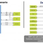
This month we’ve seen both Apple and Samsung announce their newest, flagship smart phones, and they each have an incredible number of sensors and components included like: Continue reading “What’s New with the I3C Standard”
Design for Manufacturability Analysis for PCB’s

Chip designers are familiar with the additional physical design checking requirements that were incorporated into flows at advanced process nodes. With the introduction of optical correction and inverse lithography technology applied during mask data generation, and with the extension of a 193nm exposure source to finer resolution dimensions, the traditional design rule checking (DRC) step was augmented with EDA tools that analyzed layout data to assess the fidelity of the final wafer-level structures to the original design. These algorithms were incorporated into checking tools described as providing Design for Manufacturability (DFM) support. (Parenthetically, EDA tools have also been developed to actively modify layout design data to reduce the “critical areas” that could contribute to yield loss, known as Design for Yield (DFY) modifications.)
DFM analysis has become increasingly important in the printed circuit board (PCB) design domain, as well. The scope of DFM analysis is significantly different for PCB design than chip design — PCB manufacture involves both bare board fabrication/test and subsequent component assembly. As a result, the DFM analysis for PCB design is an intricate interaction between Design for Fabrication (DFF) and Design for Assembly (DFA) requirements.
Examples of DFM checks for PCB design are illustrated below. The first depicts an “acid etch trap”, an area that may retain etchant longer than intended, resulting in open connections. The second figure highlights a design “sliver”, which is susceptible to detaching during the overall assembly flow, with the possibility of re-depositing and shorting distinct connections. Other examples include a trace routed through a solder mask opening created for a test point, or an analysis of the board stack-up thickness to via size aspect ratio to evaluate the drilling requirements and costs. These layout topologies are DRC clean, but represent additional risks during volume PCB manufacturing.
I recently had the opportunity to chat with Hemant Shah, Product Management Group Director for the Allegro PCB products at Cadence, about the expanding role of DFM for PCB design. Hemant impressed upon me the unique nature of this checking flow, as compared to IC design:
- PCB project development schedules are extremely aggressive
As a result, DFM analysis for PCB design needs to be an integral part of the design environment, with interactive results available for review.
- DFM analysis for PCBs requires access to the full board stack-up, layout, and component database.
Traditionally, multiple file formats have been used to represent the fabrication and assembly release data — e.g., Gerber drawings, CNC drill instructions, test specifications. The suite of DFM checks requires visibility into all PCB data, again necessitating integration with the design platform. (Hemant noted that the emerging IPC 2581 standard will be the comprehensive PCB release-to-manufacturing format for final analysis — please refer to www.IPC2581.com for more info.)
- PCB assembly introduces unique DFM analysis checks, beyond the IC realm.
The PCB Bill of Materials (BoM) is represented by a component library database, reflecting the schematic symbol, pad footprint, logical-to-physical correspondence, and 3D dimensional models. This library data is fundamental to DFA checking. For example, the automated optical inspection (AOI) head requires unobstructed visibility for (post-reflow) analysis of component placement/attach and detection of solder quality defects.
Hemant indicated that Cadence has addressed DFM analysis for PCBs with a new technology – the DesignTrue DFM – that is integrated into the Allegro Printed Circuit Design platform to provide real-time in-design DFM checks as the design is created.
“PCB layout designers routinely apply interactive DRC checking within Allegro. We have expanded that capability with DesignTrue DFM analysis, which incorporates over 2000 manufacturing rules. Layout designers can quickly get DFM results directly in Allegro, and evaluate them in the DRC Viewer.”, Hemant said.
Unlike the pass/fail nature of DRC rules, viewer support for DFM rules requires additional features. In addition to simply fixing DFM rule violations, layout designers can flag DFM results, assign a severity, and generate reports for broader review by the engineering team.
“How are these DFM rules developed, as part of design enablement?”, I asked.
Hemant replied, “The enablement team uses the familiar Allegro Constraints Manager interface to manage DFM rules. The rule values are commonly a combination of data from the PCB fabrication/OSAT and a customer-defined ruleset. Customers seeking multiple sourcing options may wish to establish their own encompassing rules. There is also the capability to define additional rules, beyond the 2000+ currently built into DesignTrue DFM.”
“Are DFM rules computationally expensive, especially for interactive checking?”, I inquired.
“There are seven different rule categories in DesignTrue DFM.”, Hemant indicated. Examples include: surface versus inner layer rules, rigid versus flex rules, stack-up and drill specifications, trace + via + soldermask + silkscreen rules,.
Hemant continued, “Layout designers can optimize their performance throughput by selecting specific checking tasks and/or restricting the analysis to specific regions.”
Design for Manufacturability analysis is no longer strictly part of the release handoff to the PCB fabricator, but has become a critical step in the PCB design phase. The interactive DRC checks in the PCB platform are expanding to include DFM checks, as well. The Cadence Allegro PCB DesignTrue DFM technology feature is indicative of this PCB design methodology trend — for more information on DesignTrue DFM, please follow this link.
-chipguy
Emulation Methodology for Drones and Other Video-Intensive Multimedia SoCs
What do drones, augmented reality devices, and 4K UHD TV have in common? They all include complex system-on-chips (SoCs) that must encode and decode, in real-time, data for increasingly higher definition video content. Verifying that these SoC designs are functionally correct is quite complex, but they must also function efficiently in the context of the entire system, so verifying the hardware and software too is essential. An emulation-based methodology is by far the most effective and efficient way to successfully accomplish these tasks.
Let’s take a look at the verification requirements and various verification methods design teams employ for verifying video-intensive multimedia SoCs. We’ll then examine how an emulation methodology was effectively applied to verify an SoC in one of the fastest-growing segments in the multimedia market: drones.
Challenges of Verifying Multimedia SoCs
It is not a trivial task to verify the video capture circuitry, data collection components, and streaming video essential to multimedia devices. As well, debugging is not straightforward for any type of multimedia SoC. There is a vast amount of data generated; and while video artifacts and audio glitches may be easily detectable by human eyes and ears, they are harder to spot in a waveform or database.
A few companies offer simulation acceleration IP, but this IP provides little help when verifying an SoC design with embedded software running on the full hardware design. Outside of emulation, there has not been any other way to do system-level verification of the software of a UHD-4K SoC, for example, without resorting to implementing the SoC on an FPGA prototyping system. However, FPGA prototyping is only useful if the hardware design is stable and relatively bug free. So, if the hardware is still a moving target, then the software team cannot get started until it is completed.
Although there is verification IP for UHD-4K, it is very difficult to create a simulation testbench representing the UHD-4K stimulus to put through the design. Also, with simulation-based approaches, there is an absence of efficient, built-in, system-level applications for displaying and analyzing the UHD-4K output. As well, UHD-4K verification methods that depend on simulation testbenches typically do not use real-world stimulus files.
Emulating a Multimedia Device
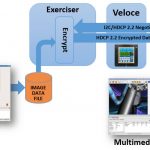
To effectively perform verification for a multimedia SoC, there must be a virtual audio-visual device to generate or receive/display UHD-4K streams to and from the design under test (along with HDCP 2.2 encrypt/decrypt). This allows teams to verify and debug the SoC pre-silicon in a software-based environment, providing both user flexibility and a high level of performance.
UHD-4K verification solutions for use with hardware emulation meet these needs (Figure 1). With the UHD-4K protocol running as a software model on an emulator, engineers can use system-level applications to drive the verification and debug process from a PC or workstation. Now, instead of having to painstakingly build a testbench to create a UHD-4K stimulus, users can simply grab an ordinary video file, even a pre-existing AVI (or WAV, TIFF, or BMP) file off the internet, and auto-convert it into a UHD-4K stream.
Figure 1 – Virtual Emulation Environment
Auto-generating a protocol-compliant UHD-4K stream saves time and risk since it eliminates the need to validate conversion compliance. The UHD-4K stream content is user-controllable by selecting a preferred pixel format or other parameters, and the UHD-4K output is compliant. Setting up the stimulus can be done in a wizard or command line, including scripting multiple stimuli.
Figure 2 – Verification of UHD Multimedia Devices
Having auto-converted the video file into UHD-4K, the UHD-4K protocol software plays the resultant stream into the DUT running on the emulator. The emulator then extracts and displays the audio-video output from the DUT and supports pixel-level graphical debugging of that displayed content; tracing particular streams or frames in detail, with video and audio.
An AVI can be exported from the DUT output to verify that it plays as expected in a real-world user application; such as Windows® Media Player. This allows the human eye to pick up errors in AV content far more efficiently than stepping manually through waveforms. Users can still zoom-in to the image to see pixel data and also examine audio detail or export the data for step-by-step waveform debugging if needed.
To facilitate debug, a programming interface can be used to export the display stream database and validate pixel data by comparing the actual against the expected outcome. If a problem is found, the log data can be output, showing content and time, so engineers can trace back on the emulator to identify what else was occurring at the moment of an error that might have caused the problem.
Debug can be a live process, capturing DUT output directly into a display and debugging on-the-fly to analyze and fix a problem immediately, or it can be captured into a database for subsequent debug. In batch mode, automated regression testing can be performed and may also be scripted for increased efficiency and productivity.
Let’s take a look at the rapidly growing drone market and how the right emulation methodology helps teams quickly bring drone innovations to market.
Invasion of the Drones
The drone market has a mega-appetite for electronics and is one of the fastest growing multimedia market segments. A recent report from BI Intelligence estimates that the investment in drone powered solutions will reach over $12bn by 2021 (Figure 3).
Figure 3- Drone Hardware Investment
With drones being applied to military, agriculture, search and rescue, broadcast and leisurely use, the drone market is getting ever more competitive. To stay ahead of the curve, drone companies are integrating high-definition video and other features into their SoCs. They are also increasingly turning to emulation for not only verifying the SoCs function properly but also for early software validation. Here are the top four reasons why they are turning to emulation methods:
[LIST=1]
Case Study: SoC Solutions for Drone Application
A Veloce customer in China creates SoC solutions for drone applications. They decided to purchase a Veloce emulation system in 2017 for the verification of their complex video chips. They did not have just one design to run on emulation, they had five unique multimedia designs that needed verification. The design sizes ranged from 15MG to 25 MG, and emulation performance was the critical factor in their decision to purchase Veloce. Multiple video protocol standards were used: HDMI, eDP and MIPI CSI-2. By using Veloce, this customer found multiple bugs in both their DUT (RTL) and firmware that would have been very difficult to find without an accelerated verification environment.
Figure 4 – Verification of Drone Application SoC
Conclusion
With all these new standards coming out and new multimedia capabilities, even more companies are going to need emulation to churn through the masses of data. The Veloce VirtuaLAB Multimedia application reduces the risk for UHD-4K and HDMI developers by allowing them to use a virtual environment to eliminate the fault errors that could occur in a final product at the pre-silicon stage. Virtualization increases verification productivity by making emulator resources available 24/7 from anywhere in the world and by significantly reducing the time to set up and run new projects.
To learn more about the challenges of the multimedia market, and how an emulation-based verification methodology offers design teams a significant advantage—please download the whitepaperDrones, Augmented Reality, UHD TV – High-End Video SoCs Need Emulation.
High-Speed Equivalence Checking

Following on product introductions for simulation and prototyping, physical verification and implementation earlier in the year, Anirudh Devgan (Exec VP and GM at Cadence), the king of speed and parallelism has done it again, this time with logic equivalence checking (LEC). Cadence recently announced an advance to their well-known conformal LEC with a new Smart LEC.
First, some background on LEC for those who started design relatively recently. Back in the mists of time when logic synthesis was becoming popular, a question asked by many design team was how they could trust that synthesis didn’t make mistakes in translating from RTL to gate-level design. Back then one answer was to repeat RTL verification regressions at the gate level. But of course that was very slow and might still miss bugs that weren’t exposed in those regression suites. Today some amount of gate-level testing is making a comeback for other reasons but would be laughably ineffective for comprehensive RTL to gate equivalence checking.
Back in 2003 Cadence acquired a private company called Verplex who had built a tool to answer this problem (then called Conformal LEC, now Conformal EC), approaching the problem of checking equivalence between RTL and synthesized gate-level netlist in a different way, through formal verification. A formal equivalence check promised complete verification of logic equivalence, unlike simulation and could complete proving in relatively modest time, again unlike simulation. It took a little work to setup but quickly became popular and a de-facto part of the implementation flow where it was also used at ties to verify the logical correctness of implementation ECOs.
Synopsys had similar technology in Formality, but users raised a common concern – if I want to check the output of a tool from company X, do I really want to use a tool also from that same company or would I rather use a tool from a competing company? Fair or not, this thinking was widespread, contributing to Conformal leadership in this domain and arguably the first real commercial success for formal technology in production design flows.
As the technology became more embedded and more proven in flows, designers felt more comfortable using more aggressive synthesis options where before it would have been very challenging to validate the equivalence of before and after synthesis behavior in any comprehensive way.
Of course it wasn’t all plain sailing for formal-based proofs either. This was especially true around datapath components and optimizations. Validating multipliers, carry-save transformations and even more tricky blended operations (multiply-accumulate for example) can’t just be thrown at standard LEC algorithms. These required specialized approaches, and specialized user-directed scripting where needed.
All such problems were conquered one way or another, but over time the setup recipes and thus scripting to run LEC became more complex and required more expert guidance both within companies and from tool providers. A natural progression perhaps, but as designs get bigger, there was a natural desire to be able to parallelize verification, yet making that truly streamlined was hampered by all these complex user-defined recipes with multiple proof strategies.
Enter Conformal Smart LEC. This will now automatically partition a design with what Cadence calls adaptive proof technology which will assign appropriate proof strategies to different parts of the design, then launch those partitions across multiple machines/CPUs for parallel proving. The platform still supports scripting but notably, according to Kam Kittrell (Product management group director, Digital & Signoff Group at Cadence), Smart LEC has been able to run large designs with the default script rather than previous complex scripts (making setup much easier). And even using that default script it has been able to complete proofs 4X faster than the previous approach on a cited customer example. Cadence asserts that the tool can transparently scale up to run on 100s of CPUs (no script changes required) and that 20X+ improvements in runtime are possible.
You can learn more about Conformal Smart LEC HERE.
Portable Stimulus Standard, What’s New from Cadence

I’ve been hearing about the Portable Stimulus Standard (PSS) since DAC 2016, so it’s helpful to get an update from EDA vendors on what their involvement level is with this emerging standard and how they see it helping design and verification engineers. Earlier in September I scheduled a conference call with Cadence and spoke with Sharon Rosenberg about the state of PSS at Cadence. What follows is my Q&A session.
Continue reading “Portable Stimulus Standard, What’s New from Cadence”
CDNLive Boston Keynote Address Highlights Emergence of Silicon Photonics

I had the pleasure of being able to attend the CDNLive event held in the Boston, MA area last month and I was pleasantly surprised to see that Cadence highlighted Silicon Photonics as one of its Keynote topics. MIT Professor Duane Boning gave an excellent overview of the current state of silicon photonics and why he believes it is time for the electrical engineering community to learn about this important technology. In Professor Boning’s presentation, he made the claim that silicon photonics has become “Interesting, Convergent and Designable”.
Professor Boning noted silicon photonics as interesting because it is bringing new functionality and capabilities to the market that are tied to real business. It is predicted that by the year 2025, the silicon photonics IC market will have reached $108 Billion with a little over half of that coming from the DataCom and Telecom industries. The data centers are pushing for greater bandwidth density while simultaneously desiring lower signal latency and lower overall power consumption. Silicon photonics technology gives them all three without compromise. Moving the photonic components from the active optical cables (AOCs) onto the server boards and eventually integrated with the processors themselves will drive IC volumes up dramatically. That will give the data centers the last important part of the equation, which is reduced cost. How many technologies give you more bandwidth density, less latency and less power consumption while also driving down costs?
The second biggest silicon photonics market will be in the area of sensors. This market is projected to grow to $41.4 billion by 2025. With the advent of the internet of things (IoT), sensors will be literally everywhere. One of the biggest drivers for volume ICs in sensing will be the healthcare industry where photonics will be combined with fluidics and electronics to deliver the long-awaited lab-on-a-chip. The lab will literally be brought to a patient’s bedside in the pocket of a technician. These ICs will be one-time use which means really high volumes and that will help to drive down IC costs. Sensing doesn’t stop at healthcare however. Sensors will also be heavily used in industrial and military applications as well.
One specialized form of sensor is used for imaging and will be especially useful for the autonomous vehicle market in the form of LIDAR (Light Detecting and Ranging). The market for LIDAR based imaging and display systems ICs is projected to reach $4.5 billion by 2025. Given all these applications it is no small wonder that Cadence Design Systems has hopped onto the photonics bandwagon.
The second thing Professor Boning noted was that silicon photonics is convergent. By that he explained that CMOS electronics and silicon-based photonics fabrication technologies have evolved toward each other to enable monolithic electro-photonic solutions.
There are currently two main approaches for monolithic integration. The first involves integrating photonics into the front-end-of-line (FEOL) layers while the second integrates photonics into the back-end-of-line (BEOL) layers. Both have their merits and their detractors. The good news is that no matter which way the industry goes, in both cases, photonics is sharing wafer processing, equipment and materials with standard CMOS. That means that silicon photonics can be added rapidly to commercial CMOS product lines with relatively low capital investment on the part of the foundries. We’ve already seen announcements from several of the production foundries adding silicon photonics to their offerings (Global Foundries, TowerJazz, TSMC/Luxtera, ST Microelectronics, and AMS).
Also along the convergence path is the fact that photonics is mirroring electronics in its approach to design flow and design automation tools. The photonics ecosystem has been working for almost a decade now on establishing a common set of photonic device building blocks from which photonic circuits can be assembled. These building blocks are common in multiple foundry process design kits (PDKs) and can be used to design and map photonic circuits from one foundry to another through a process PhoeniX Software calls photonic synthesis.
Professor Boning also showed a slide of the recently announced Cadence, Lumerical, PhoeniX EPDA (electronic/photonic design automation) flow and noted that two of the break-out sessions presented at this CDNLive event were about the design and manufacturing of silicon photonics (courtesy Lumerical Solutions and Analog Photonics).
The last point Professor Boning made was that silicon photonics is now “designable”. As just mentioned, the design flow is mimicking that of electronics and now includes tools from multiple photonic and electronic design automation vendors. Design tools are now available for photonic device simulation, abstraction of photonic component behavior into compact models, photonic circuit simulation, automated layout generation including parameterized cells (pcells), DRC (design rule checking) and emerging LVS (layout vs schematic) flows. These tools and flows are supported by multiple foundries with qualified PDKs. More recently new flows for integration of digital and analog/mixed-signal electronics with photonic is now being put into place for systems-in-package (SiP) configurations (see Cadence Photonic Summit 2017).
For those interested in seeing where photonics is going and the kinds of capabilities that will be coming online in the next decade I refer you to the IPSR (Integrated Photonic Systems Roadmap) that can be found at http://photonicsmanufacturing.org/.
In summary, Cadence has done an excellent job of keeping their customers abreast of the latest evolving technologies and their CDNLive events are definitely worth attending. If you haven’t been to one in a while I would highly recommend you attend one to see what the world is up to. This one really shined some light (laser light that is) on the future.
See Also:
CDNLive website
How to Avoid Jeopardizing SoC Security when Implementing eSIM?
Smart card business is now more than 25 years old, we can assess that the semiconductor industry is able to protect the chips used for smart card or SIM application with a very good level (unfortunately, it’s very difficult to get access to the fraud percentage linked with smart cards, as bankers really don’t like to communicate on this topic!). The various techniques and algorithms to protect chips against attacks have proven to be efficient, but just keep in mind that security experts like Alain Merle (Dr of security with CEA-LETI) evaluate the weight of good security level to be 50% of the IC total cost, for a smart card or SIM.
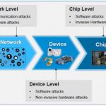
Now the problem is moving from a single chip dedicated to SIM (or smart card), that we know how to best protect against fraud, to the embedded version of this chip, integrated as one of the functions integrated into an application processor SoC. We are talking about embedded SIM (eSIM) and any function supporting mobile payment being integrated into a SoC targeting mobile, IoT and automotive applications. How to best protect it from the various possible attacks?
Synopsys has developed pre-verified DesignWare ARC Secure IP Subsystem to provide a trusted hardware and software SoC environment. This subsystem is created around the new ARC SEM110, or ARC SEM120D (the D stands for DSP extension).
The ARC SEM is an ultra-low power security processor with SecureShield technology, enabling creation of Trusted Execution Environment (TEE) and protecting against side-channel attacks and data breaches. Synopsys offers cryptography options to accelerate encryption for a range of algorithms including AES, SHA-256, RSA and ECC. To protect the instruction code and data, the code and data are stored encrypted in the memories, embedded or external and secured instruction and data controllers provide external memory access protection and runtime tamper detect. This secure external memory controller is a licensable product option.
SoC architect can implement security at S/W level only, using subsystem software including NIST-validated crypto library (for non US: NIST stand for National Institute of Standard Technology), secure boot and SecureShield runtime library (embARC), or complement with H/W engines like Symmetric Crypto/Hashing or Asymmetric Crypto coprocessors.
ARC SEM110 and SEM120D are well suited for secure element implementations, like eSIM or eUICC. UICC being the new generation of SIM, able to support multiple applications, like USIM (to identify you and your phone plan to your service provider) or ISIM (to secure mobile access to multimedia services, and non-telecom applications such as payment).
At the chip level, the number of potential attacks is vast, as we can see on the above picture. During communication, we can mention sniffing of sensitive data like passwords, direct remote attacks via backdoors or indirect via remotes nodes. Software is well-known for the sensibility to malware (viruses or rootkits), but it can also a vector to exploit buffer/stack overflows, or for privilege level tampering. Hardware can be sensible to invasive attacks like decapsulation or probing (even if these can also be used by analyst!) and non-invasive like side-channel of access to the inside by using debug ports.
ARC SEM security processor has been designed to be immune to these attacks, hardware or software. SecureShield offers multiple isolated execution context. Side-channel protection is realized by defining an uniform instruction timing, and via timing and power randomization. The processor pipeline is made tamper-resistant by in-line instruction, data and address scrambling. Error detection and parity has been implemented for memories and registers. Even the debug functionality has been secured to prevent non-invasive side-channel attacks. Integrated watchdog timer detects system failures, including tampering.
You shouldn’t be surprised to learn that ARC SEM has been the analysts’ choice in 2016 for the Linley Group Best Processor IP award!
The ARC Secure IP Subsystem is available now.
- Learn more about DesignWare ARC Subsystems
- Learn more about ARC SEM Processors and SecureShield technology
- Learn more about Synopsys DesignWare Security IP Solutions
From Eric Esteve from IPnest