Designing at 7nm is a big deal because of the costs to make masks and then produce silicon that yields at an acceptable level, and Silicon Creations is one company that has the experience in designing AMS IP like: PLL, Serializer-Deserializer, IOs, Oscillators. Why design at 7nm? Lots of reasons – lower power, higher speeds, longer battery life.
Continue reading “Silicon Creations talks about 7nm IP Verification for AMS Circuits”
DSP-Based Neural Nets
You may be under the impression that anything to do with neural nets necessarily runs on a GPU. After all, NVIDIA dominates a lot of what we hear in this area, and rightly so. In neural net training, their solutions are well established. However, GPUs tend to consume a lot of power and are not necessarily optimal in inference performance (where learning is applied). Then there are dedicated engines like Google’s TPU which are fast and low power, but a little pricey for those of us who aren’t Google and don’t have the clout to build major ecosystem capabilities like TensorFlow.
Between these options, lie DSPs, especially embedded DSPs with special support for CNN applications. DSPs are widely recognized to be more power-efficient than GPUs and are often higher performance. Tying that level of performance into standard CNN frameworks like TensorFlow and a range of popular network models makes for more practical use in embedded CNN applications. And while DSPs don’t quite rise to the low power and high performance of full-custom solutions, they’re much more accessible to those of us who don’t have billion dollar budgets and extensive research teams.
CEVA offers a toolkit they call CDNN (for Convolutional Deep Neural Net), coupling to their CEVA-XM family of embedded imaging and vision DSPs. The toolkit starts with the CEVA network generator which will automatically convert offline pre-trained networks / weights to a network suited to an embedded application (remember, these are targeting inference based on offline training). The convertor supports a range of offline frameworks, such as Caffe and TensorFlow and a range of network models such as GoogLeNet and Alex, with support for any numbers and types of layers.
The CDNN software framework is designed to accelerate development and deployment of the CNN in an embedded system, particularly though support functions connecting the network to the hardware accelerator and in support of the many clever ideas that have become popular recently in CNNs. One of these is “normalization”, a way to model how a neuron can locally inhibit response from neighboring neurons to sharpen signals (create better contrast) in object recognition.
Another example is support for “pooling”. In CNNs, a pooling layer performs a form of down-sampling, to reduce both the complexity of recognition in subsequent layers and the likelihood of over-fitting. The range of possible network layer types like these continues to evolve, so support for management and connection to the hardware through the software framework is critical.
This framework also provides the infrastructure for these functions you are obviously going to need in recognition applications, like DMA access to fetch next tiles (in an image, for example), store output tiles, fetch filter coefficients and other neural net data.
The CDNN hardware accelerator connects these functions to the underlying CEVA-XM platform. While CEVA don’t spell this out, it seems pretty clear that providing a CEVA-developed software development infrastructure and hardware abstraction layer will simplify delivery of low-power and high-performance for embedded applications on their DSP IP. An example of application of this toolkit to development of a vision / object-recognition solution is detailed above.
Back to the embedded / inference part of this story. It has become very clear that intelligence can’t only live in the cloud. A round-trip to the cloud won’t work for latency-sensitive applications (industrial control and surveillance are a couple of obvious examples) and won’t work at all if you have a connectivity problem. Security isn’t exactly enhanced in sending biometrics or other certificates upstream and waiting for clearance back at the edge. And the power implications are unattractive in streaming the large files required for CNN recognition applications to the cloud. For all these reasons, it has become clear that inference needs to move to the edge, though training can still happen in the cloud. And at the edge, GPUs characteristically consume too much power while embedded DSPs are battery-friendly. DSPs benchmark significantly better on GigaMACs and on GigaMACs/Watt, so it seems pretty clear which solution you want to choose for embedded edge applications.
To learn more about what CEVA has to offer in this area, go HERE.
IoT Security Hardware Accelerators Go to the Edge
Last month I did an article about Intrinsix and their Ultra-Low Power Security IP for the Internet-of-Things (IoT). As a follow up to that article, I was told by one of my colleagues that the article didn’t make sense to him. The sticking point for him, and perhaps others (and that’s why I’m writing this article) is that he couldn’t see why you would want hardware acceleration for security in IoT edge devices. He wasn’t arguing the need for security. He was simply asking why you would spend the extra hardware area in a cost-sensitive device when you could just use the processor you already have in the device to do the work in software.
I thought this was a good question and one that needed more than a flippant answer from me, so I went back to Intrinsix and had an interesting discussion with Chuck Gershman, director of strategic development at Intrinsix. It turns out the short answer is “power.” Edge devices spend a large percentage of their life not doing much. Many of the newest edge devices run off the tiniest of batteries and use energy harvesting from vibrations, pressure, light, etc. to fuel themselves. To do this, however, they must literally be able to shut themselves down for long periods of time.
So, how do security accelerators help? Well, most IoT edge devices that use their CPUs for security tasks don’t really shut down. They go into a sleep mode that keeps system registers alive so that they don’t lose device state. If you lose device state, the device must do a secure boot when it is time to wake up, and that takes CPUs both time and energy.
Intrinsix has shown that by using their hardware accelerated IP, they can fully shut down the device and then do a secure reboot in milliseconds instead of multiple seconds it takes a CPU to do the same thing. By using a dedicated hardware accelerator, they can boot the system up to 800 times faster, and the amount of power saved by being fully shut down instead of simply sleeping can lead to a 1000X power reduction and up to 10X better battery life.
Not to be totally rebuffed, my colleague then made the point that we were talking about IoT edge devices that were supposed to cost in the sub $1 / device range (in some cases in the pennies per device range). Hardware accelerators implied bigger die which means higher costs. In one sense my colleague was correct. It’s well known that cloud servers and IoT network hubs are expected to have lots of encrypted traffic as the cloud servers could be dealing with hundreds of network hubs, and the network hubs could be dealing with thousands of edge devices. One would expect to see dedicated security hardware in these devices to handle all the secure connections. The edge device, however, is likely only to be talking to just a few or maybe only one network hub.
Time for another discussion with Chuck who was all too happy to explain that the beauty of the Intrinsix security IP was that it was highly scalable. It turns out when Intrinsix designed their IP, they used an architecture that let them use configurable parallel computing for the security features. This means that they can optimize the design to meet different power, performance, and area (PPA) trade-offs while still giving you the benefit of having hardware acceleration.
So, you can still get the power benefits provided by the accelerators while having a minimal area penalty (which could be insignificant depending on the silicon technology used, pinout and package). And, since the IP is configurable, you can optimize the IP for whatever work load the device is expected to see. For network hubs and servers that means you can significantly boost their performance by adding more parallel compute lanes in the IP.
Last statement from my doubting colleague, was “Ok, so it sounds like I have to be a security guru to know how to optimize this IP to make the implied trade-offs”. For this one, I already knew the answer, which was, “no, you don’t.” Intrinsix is a design services firm that has the platforms, process, and people required to ensure first-turn success of your semiconductor project. They already have security expertise in-house and the necessary knowledge to optimize the IP for you. You tell them what you are trying to do and they can generate a fully optimized security IP for the job that is ready to drop into your ASIC. And… If you so desire, they can also help you to embed the IP into your ASIC or do the entire ASIC as well.
So, for those readers who had the same doubts as my colleague, I hope this article has cleared things up. Of course, if you want more details the Intrinsix team will be happy to talk to you.
If you want to learn more about Intrinsix and their IoT offerings, you can find them online at the link below. You may also want to download their IoT eBook.
See also:
eBook: IoT Security The 4[SUP]th[/SUP] Element
Intrinsix Fields Ultra-Low Power Security IP for the IoT Market
Intrinsix Website
Arm TechCon Preview with the Foundries!
This week Dr. Eric Esteve, Dr. Bernard Murphy, and I will be blogging live from Arm TechCon. It really looks like it will be a great conference so you should see some interesting blogs in the coming days. One of the topics I am interested in this year is foundation IP and I will tell you why.
During the fabless transformation of the semiconductor industry, semiconductor IP became a key enabler with EDA tools and ASIC services. Today, as non-traditional chip companies start designing chips from scratch, Foundation IP (SRAM, Standard Cells, and I/Os) from leading IP companies will again be front and center and when you want to know the latest about Foundation IP you talk to the foundries, absolutely.
In case you did not know, one of our leading foundry executives recently moved to Semiconductor IP which will bring a whole new perspective. Kelvin Low started at Chartered Semiconductor, then GLOBALFOUNDRIES, followed by Samsung Foundry, and is now Vice President of Marketing at Arm Physical Design Group where he will soon celebrate his 20th year in semiconductors. I had lunch with Kelvin recently and he told me what to look for in regards to foundries this week at Arm TechCon which starts with a free lunch with TSMC, Cadence, Xilinx, and Arm:
Unprecedented Industry Collaboration Delivers Leading 7nm FinFET HPC Solutions
Join us for an ecosystem lunch and joint presentations from our Ecosystem partners focusing on FinFET collaboration!In the first section of this set of four sessions, you will hear how Arm® and its Ecosystem partners delivered industry-leading 7nm FinFET solutions to address applications of the High Performance Computing (HPC) segment. With the implementation complexity at small geometries and more demanding product requirements, it is imperative that the Ecosystem collaborate closely to meet the most stringent system-level performance and power targets. Speakers from TSMC®, Cadence®, Xilinx® and Arm will share details of our combined effort and discuss key challenges and future opportunities.
Transforming Markets with Arm and Intel FinFET Solutions
In the second of four sessions, extend your lunch with us to hear from Arm and Intel® on our new partnership focusing on our collaborative solutions for 10hpm and 22ffl. The second part of the sponsored session covers the joint strategy bringing Arm and Intel Custom Foundry to the ecosystem. Together, we will share our planned journey to enable smart mobile computing on these key process nodes. Speakers from Arm and Intel will also discuss co-optimization of the process technology, and how we will expand the collaboration for broader solutions.
Samsung Foundry Roadmap to Advanced FinFET Nodes
In the third of four sessions, we welcome presenters from Samsung Foundry and Arm. Samsung Foundry will showcase their latest FinFET roadmap at 14nm, 11nm and beyond, including the value proposition and target markets for their advanced nodes. Samsung and Arm will highlight the results of our collaborative efforts in this space with Arm detailing their 14LPP and 11LPP platform offering and support of the Samsung Foundry roadmap for the benefit of the ecosystem.
Arm Physical Design Solutions
In the fourth of four sessions, we invite you to close out your lunch and hear direct from Arm on our physical design solutions for the ecosystem. We will cover cross-foundry roadmaps with a focus on POPTM IP, bring new optimizations to Arm CortexTM-A cores targeting improved design turnaround time. And we have an exciting announcement for our product availability on DesignStart.
If you would like to meet us at Arm TechCon message us on SemiWiki and I will make sure it happens. You can meet me in the Open-Silicon booth #918 Wednesday morning where we will be giving away 300 copies of “Custom SoCs for IoT: Simplified”. It would be a pleasure to meet you. Or you can Download the Free PDF Version Here.
TSMC: Semiconductors in the next ten years!
The TSMC 30th Anniversary Forum just ended so I will share a few notes before the rest of the media chimes in. The forum was live streamed on tsmc.com, hopefully it will be available for replay. The ballroom at the Grand Hyatt in Taipei was filled with cameras, semiconductor executives, and security personnel.
The event started with a video about TSMC over the last 30 years followed by comments from Chairman Morris Chang. The keynotes were by Nvidia CEO Jensen Huang, Qualcomm CEO Steve Mollenkopf, ADI CEO Vincent Roche, ARM CEO Simon Segars, Broadcom CEO Hock Tan, ASML CEO Peter Wennink, and Apple COO Jeff Williams. Next was a panel discussion led by Chairman Morris Chang.
First let’s start with the jokes. Jensen Huang was supposed to go first but his presentation was not ready and Morris roasted him a bit over it. Jensen replied that it took him longer because he actually prepared for the event. Funny because it was a joke with a bit of truth to it because the other presentations were standard stock. Jensen did the best presentation which was all about AI which is in fact the future of semiconductors in the next ten years.
The best joke however was in response to a question about legal matters, if AI goes wrong who is held accountable? Morris pointed out that Steve Mollenkopf probably has the most legal experience of the group referring to Qualcomm’s massive legal challenges of late. Steve recused himself from the question of course. Even at 86 years old Morris still has a quick wit and provided most of the humor for the evening.
As I have mentioned before, AI will touch almost every chip we make in the coming years which will bring an insatiable compute demand that general purpose CPUs will never satisfy. This year Apple put a neural engine on the A11 SoC that’s capable of up to 600 billion operations per second. Nvidia GPUs do trillions of operations per second so we still have a ways to go for edge devices.
A couple of more interesting notes, the Apple-TSMC relationship started in 2010 which didn’t produce silicon until the iPhone 6 in 2014. Morris described the Apple-TSMC relationship as intense but Jeff Williams (Apple) said that you cannot double plan for the volumes of technology that Apple requires so partnerships are key. My take is that the TSMC-Apple relationship is very strong and will continue for the foreseeable future. Who else is going to be able to do business the Apple (non competing) way and still make big margins?
Jeff also predicts that medical will be the most disruptive AI application to which Morris agreed suggesting mediocre doctors will be replaced by technology. This is something I feel VERY strongly about. Medical care is barbaric by technology standards and we as a population are suffering as a result. Apple is focused on proactive medical care versus reactive which is what you see in most hospitals. Predicting strokes or heart events is possible today for example. AI enabled medical imaging systems is another example for tomorrow.
Security and privacy were discussed with Apple insisting that your data is more secure on your device than it is in the cloud. Maybe that’s why the new phones have a huge amount of memory (64-256 GB) while free iCloud storage is still only 5 GB. We use a private 1 TB cloud for just that reason by the way, our data stays in our possession. I certainly agree about security but privacy seems to be lost on millennials and they are the target market for most devices.
Bottom line: Congratulations to the TSMC support staff, this event was well done and congratulations to TSMC for an amazing 30 years. The room was filled with C level executives and a smattering of media folks like myself. It really was an honor to be there, being part of semiconductor history, absolutely.
Webinar: Optimizing QoR for FPGA Design
You might wonder why, in FPGA design, you would go beyond simply using the design tools provided by the FPGA vendor (e.g. Xilinx, Intel/Altera and Microsemi). After all, they know their hardware platform better than anyone else, and they’re pretty good at design software too. But there’s one thing none of these providers want to support – a common front-end to all these platforms. If you want flexibility in device providers, making a vendor change will force you back to an implementation restart. Which is one reason why tools like Synplify Premier from Synopsys have always had and always will have a market.
REGISTER HERE for this webinar on October 25[SUP]th[/SUP] at 10am PDT
The other reason is that a company whose primary focus is in design software, and which started and still leads design synthesis market, is likely to have an edge in synthesis QoR, features and usability over the device vendors. Of course, the physical design part of implementation still comes from the vendors, but Synplify tightly couples with these tools, not just in the sense of “you can launch Vivado from Synplify” but also in the sense that you can iteratively refine the implementation, as you’ll see soon.
As an example of what you get in synthesis from a tool in the Synopsys stable, Synplify Premier will handle optimization for state-machines (including recoding to other styles such as Gray encoding), resource-sharing, pipelining and retiming. And of course, they support DesignWare IP.
This webinar provides a fairly detailed overview of what is possible using Synplify Premier as your FPGA design front-end. Much of this will be familiar to ASIC designers or to FPGA designers already familiar with tools from device vendors. One topic is on optimal RTL coding styles, for FSMs (for optimization to the target device, to map away unreachable states, add safe recovery from invalid states or to change coding), math and DSP functions for efficient packing (for filters, counters, adders, multipliers, etc) and optimized RAM inferencing based on availability of resources (block RAMs etc).
Static timing analysis will look very familiar, except that the Synopsys constraint format is called FDC (FPGA design constraints) rather than SDC. Synplify Premier provides a nice feature to automatically create a quick set of constraints in early design to help you get through the basic flow-flush. Naturally you’ll want to work on developing real constraints (real clocks, clock groups, I/O constraints, timing exceptions, etc) before you move to physical design.
I mentioned earlier that interoperability between Synplify Premier and the vendor physical design tools isn’t just about compatibility in libraries, tech files and data passed from the synthesis tool to the vendor tool. A great example is in congestion and QoR management. These problems happen for well-known reasons – high resource utilization, over-aggressive constraints, logic packing problems and others.
One particularly important root cause can happen on Xilinx device which are multi-die (each die is known as super-logic region/SLR) on an interposer connected by super-long line (SLL) interconnects. You already know where this is going; there are only so many SLLs, which means they can be over-used (I assume there might also be reduced timing margin on SLLs). So lots of congestion and timing closure problems can happen – no news to implementation experts. What is interesting here though is that Synplify Premier can take this information from Xilinx or Intel project files and use it to drive re-synthesis to reduce congestions and timing closure problems. It also can drive many runs in parallel on a server farm so you can quickly explore different implementation strategies. That’s real and very useful interoperability.
If you’re not familiar with Synplify Premier, this should be a must-see. Remember to
REGISTER HERE for this webinar on October 25[SUP]th[/SUP] at 10am PDT
The Interface IP Market has Grown to $530 Million!
According with IPnest, the Interface IP market, including USB, PCI Express, (LP)DDRn, HDMI, MIPI and Ethernet IP segments, has reached $532 million in 2016, growing from $472 million in 2015. This is an impressive 13% Year-over-Year growth rate, and 12% CAGR since 2012!
Who integrate functions to interface a chip with others IC or connector? The answer is simply that for any application, you need to interact with another chip (DRAM, SSD, Application Processor or ASSP), or with the outside world through a connector (from HDMI to PCIe or USB). If you consider chip design, you quickly realize that two kinds of functions are ubiquitous: processing and interfacing. This consideration is comforted by their respective weight in the IP license market (before royalty). In 2016, the license only market has weighted $1930 million. The license revenues generated by processor IP (CPU, GPU, DSP) of $680 million represent 35% of the total, when the interface IP license, weighting $532 million, is 27.5%. The addition of processor and interface IP generates 62.5% of the total (license) IP market.
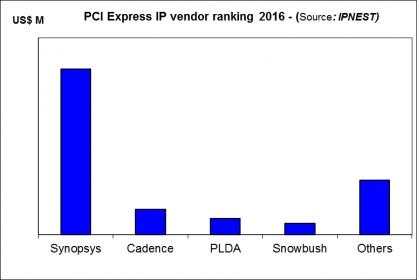
If ARM is known to be the king of the processor IP market, and consequently, thanks to royalties, of the total IP market with 48.4% market share, Synopsys is the duke. Synopsys is now the clear #2 of the design IP market, and the undisputed leader of the interface IP market, with 51% market share and over $270 million revenues. In fact, if we look at this market by segment, USB, PCI Express, etc., Synopsys is also the leader in each of these 5 IP segments: USB, PCI Express, MIPI, HDMI, DDRn, with a market share between 50% to 75%.
In the survey, IPnest is making a very comprehensive analysis, by protocol, including a ranking by IP vendor and competitive analysis, or a review of all the IP vendors active in the segment. It’s always possible to find a niche where a vendor, not necessarily leader, will enjoy good business. IPnest also analyze the market trends to predict the future adoption of a specific protocol in new applications. For example, PCI Express protocol was initially developed to support the PC, computing and networking segments. We have seen the pervasion in mobile, with Mobile Express definition in 2012, but also in storage (NVM Express) and the pervasion in automotive is now acted.
Such comprehensive analysis will help IPnest to build 5 years forecast, taking into account the growth of number of design starts including PCIe function, and also that we call “externalization factor”. The externalization factor is the augmentation of the proportion of PCIe IP being externalized, and this factor may change every year, even if the proportion of commercial IP is only growing, year after year.
Competitive analysis: IPnest propose, by protocol, a competitive analysis and a ranking, like for example for PCI Express:
Being part of the DAC IP committee and running IPnest, Eric Esteve was also the chairman of the panel “The IP Paradox” (The semiconductor industry is consolidating, and the number of potential customers is shrinking, but the IP market is still growing, in particular the interface IP market. How to explain this growth?). If we can answer this question, we will be able to more accurately forecast the IP market growth.
John Koeter, VP Marketing for Synopsys, has proposed an explanation: “We study the market and 60-70% of the IP is outsourced. When I look at IP, I think it is potentially the same size as the EDA market. EDA is fully outsourced, but IP is not there yet which means there is growth available.”IPnest 100% agree with this! If we try to model the IP market growth, we see that there is 10 to 15 years growth reserve for the IP market to be fully outsourced (assuming +/-3% value for the externalization factor).
A graphic view of the market evolution, by protocol, for 2012 to 2021:
It’s important to notice that IPnest is now the only company offering the “Design IP Report” (2015 and 2016 ranking of all the IP vendors by categories, from CPU to GPU, DSP, mixed-signal, memory compilers, libraries, interface, etc.) as Gartner has stopped to make it in 2016. IPnest is also the only analyst launching the “Interface IP survey & forecast”. In fact, this is the 9[SUP]th[/SUP] version of this report and was launched last week.
If you are interested by the Table of Content for the 2017 version of the report (2012-2016 Survey – Forecast 2017-2021), just send me a message on Semiwiki, or on Linkedin: Eric Esteve
We can also meet during ARM TechCon in Santa Clara (10/24 to 10/26), I will stay until 10/27.
Eric Esteve
GLOBALFOUNDRIES RF Leadership
“Mobile is the largest platform ever built by humanity”, Christiano Amon, Executive Vice President, Qualcomm Technologies, Inc. and President, Qualcomm CDMA Technologies speaking at the GLOBALFOUNDRIES Technologies Conference (GTC) 2017.
Continue reading “GLOBALFOUNDRIES RF Leadership”
IEDM 2017 Preview
The 63rd annual IEDM (International Electron Devices Meeting) will be held December 2nd through 6th in San Francisco. In my opinion IEDM is one of, if not the premier conference on leading edge semiconductor technology. I will be attending the conference again this year and providing coverage for SemiWiki. As a member of the press I got some preview materials today and I wanted to share some of it with you.
Leading Edge Logic
As anyone who has read my articles on SemiWiki knows I follow the latest advances in logic process technology very closely. In the Platform Technology Session there will be papers from Intel on their 10nm technology and GLOBALFOUNDRIES on their 7nm technology and I am really looking forward to these papers:
- Intel: Intel researchers will present a 10nm logic technology platform with excellent transistor and interconnect performance and aggressive design-rule scaling. They demonstrated its versatility by building a 204Mb SRAM having three different types of memory cells: a high-density 0.0312µm[SUP]2[/SUP] cell, a low voltage 0.0367µm[SUP]2[/SUP] cell, and a high-performance 0.0441µm[SUP]2[/SUP] cell. The platform features 3[SUP]rd[/SUP]-generation FinFETs fabricated with self-aligned quadruple patterning (SAQP) for critical layers, leading to a 7nm fin width at a 34nm pitch, and a 46nm fin height; a 5[SUP]th[/SUP]-generation high-k metal gate; and 7[SUP]th[/SUP]-generation strained silicon. There are 12 metal layers of interconnect, with cobalt wires in the lowest two layers that yield a 5-10x improvement in electromigration and a 2x reduction in via resistance. NMOS and PMOS current is 71% and 35% greater, respectively, compared to 14nm FinFET transistors. Metal stacks with four or six workfunctions enable operation at different threshold voltages, and novel self-aligned gate contacts over active gates are employed. (Paper 29.1, “A 10nm High Performance and Low-Power CMOS Technology Featuring 3[SUP]rd[/SUP]-Generation FinFET Transistors, Self-Aligned Quad Patterning, Contact Over Active Gate and Cobalt Local Interconnects,” C. Auth et al, Intel)
- GLOBALFOUNDRIES (GF): GF researchers will present a fully integrated 7nm CMOS platform that provides significant density scaling and performance improvements over 14nm. It features a 3[SUP]rd[/SUP]-generation FinFET architecture with SAQP used for fin formation, and self-aligned double patterning for metallization. The 7nm platform features an improvement of 2.8x in routed logic density, along with impressive performance/power responses versus 14nm: a >40% performance increase at a fixed power, or alternatively a power reduction of >55% at a fixed frequency. The researchers demonstrated the platform by using it to build an incredibly small 0.0269µm[SUP]2[/SUP] SRAM cell. Multiple Cu/low-k BEOL stacks are possible for a range of system-on-chip (SoC) applications, and a unique multi-workfunction process makes possible a range of threshold voltages for diverse applications. A complete set of foundation and complex IP (intellectual property) is available in this advanced CMOS platform for both high-performance computing and mobile applications. (Paper 29.5, “A 7nm CMOS Technology Platform for Mobile and High-Performance Compute Applications,”S. Narasimha et al, Globalfoundries)
Silicon Photonics
Silicon Photonics is an area of great interest in the industry today and in my cost modeling business I am getting a lot of interest in Silicon Photonics costs. Session 34 will focus on Silicon Photonics.
Silicon Photonics: Current Status and Perspectives (Session #34) – Silicon photonics integrated circuits consist of devices such as optical transceivers, modulators, phase shifters and couplers, operating at >50 GHz for use in next-generation data centers. This session describes the latest in photonics IC advances in state-of-the-art 300mm fabrication technology; integrated nano-photonic crystals with fJ/bit optical links; and advanced packaging concepts for the specialized form factors this technology requires.
- “Developments in 300mm Silicon Photonics Using Traditional CMOS Fabrication Methods and Materials,” by Charles Baudot et al, STMicroelectronics
- “Reliable 50Gb/s Silicon Photonics Platform for Next-Generation Data Center Optical Interconnects,” by Philippe Absil et al, Imec
- “Advanced Silicon Photonics Technology Platform Leveraging the Semiconductor Supply Chain,” by Peter De Dobbelaere, Luxtera
- “Femtojoule-per-Bit Integrated Nanophotonics and Challenge for Optical Computation,” by Masaya Notomi et al, NTT Corporation
- “Advanced Devices and Packaging of Si-Photonics-Based Optical Transceiver for Optical Interconnection,” by K. Kurata et al, Photonics Electronics Technology Research Association
Nanowires
With FinFETs coming to the end of it’s scaling potential nanowires are garnering a lot of interest as the next generation technology. In session 37 there will be a couple of papers on nanowires incuding:
First Circuit Built With Stacked Si Nanowire Transistors: As scaling continues, gate-all-around MOSFETs are seen as a promising alternative to FinFETs. They are nanoscale devices in which the gate is completely wrapped around a nanowire, which serves as the transistor channel. Nanosheets, meanwhile, are sheets of arrays of GAA nanowires. A talk by Imec and Applied Materials will describe great progress in several key areas to make vertically stacked GAA nanowire and/or nanosheet MOSFETs practical. The team built the first functional ring oscillator test circuits ever demonstrated using stacked Si nanowire FETs, with devices that featured in-situ doped source/drain structures and dual-workfunction metal gates. An SiN STI liner was used to suppress oxidation-induced fin deformation and improve shape control; a high-selectivity etch was used for nanowire/nanosheet release and inner spacer cavity formation with no silicon reflow; and a new metallization process for n-type devices led to greater tunability of threshold voltage. (Paper 37.4, “Vertically Stacked Gate-All-Around Si Nanowire Transistors: Key Process Optimizations and Ring Oscillator Demonstration,” H. Mertens et al, Imec/Applied Materials)
Conclusion
These papers are just a sampling of what will be presented that are of interest to me. I highly recommend attending IEDM for anyone interested in staying current on the state-of-the art.
How standard-cell based eFPGA IP can offer maximum safety, flexibility and TTM?
Writing a white paper is never tedious, and when the product or the technology is emerging, it can become fascinating. Like for this white paper I have written for Menta “How Standard Cell Based eFPGA IP are Offering Maximum Flexibility to New System-on-Chip Generation”. eFPGA technology is not really emerging, but it’s fascinating to describe such a product: if you want to clearly explain eFPGA technology and highlight the differentiators linked with a specific approach, you must be subtle and crystal clear!
Let’s assume that you need to provide flexibility to a system. Before the emergence of eFPGA, the only way was to design a FPGA, or to add a programmable integrated circuit companion device (the FPGA) to an ASIC (the SoC). Menta has designed a family of FPGA blocks (the eFPGA) which can be integrated like any other hard IP into an ASIC. It’s important to realize that designing eFPGA IP product is not just cutting a FPGA block that you would deliver as is to an ASIC customer.
eFPGA is a new IP family that a designer will integrate into a SoC, and in this case, every IP may be unique. Menta is offering to the SoC architect the possibility to define a specific eFPGA where logic and memory size, MAC and DSP count are completely customizable, as well as the possibility to include inside this eFPGA certain customer defined blocks.
Menta has recently completed the 4[SUP]th[/SUP] generation of eFPGA IP (the company has been started 10 years ago) and the vendor offers some very specific features to build a solution more attractive than these offered by the competition. Why is Menta eFPGA IP more attractive? We will see that the solution is more robust, the architecture provides maximum flexibility and the porting to different technology node is safer and faster, allowing faster time-to-market. This solution also allows smoother integration in the EDA flow, including easier testability.
When most of FPGA are programmed via internal SRAM (as well as most of eFPGA), Menta has decided to rely on D-Flip-Flop for the programming. This approach makes the eFPGA safer, and for two reasons. At first, when SRAM are known to be prone to Single Upset Event (SUV), DFF show a better SUV immunity. The reason is very simple, the most significant factor is the physical size of the transistor geometries (smaller means less SEU energy required to trigger them), and the DFF geometry is larger than the equivalent storing cell in SRAM. That’s why Menta eFPGA architecture is well suited for automotive application, for example.
The second argument for a better safety is that designing programming SRAM will be based on a full custom approach, requiring new characterization every time you change technology node, when Menta is using DFF from a standard cell library, or pre-characterized, by the foundry or the library vendor.
In the white paper, you will learn why Menta eFPGA architecture eFPGA provide maximum flexibility, as the designer can include logic, memory, and internal I/O banks, infer pre-defined (by Menta) DSP primitives or include custom (made by the designer) DSP blocks.
Really, the key differentiator is linked with the decision to base eFPGA architecture only on standard blocks. The logic is based on standard cells, as well as the DSP primitives and internal I/O banks. Once Menta has validated eFPGA IP on a certain technology node, any customer defined eFPGA will be correct by construction. When a “mega cell” is only made of standards cells characterized by the foundry or the library vendor, the direct two consequences are safety and ease of use.
Safety because there is no risk of failure when using pre-characterized library and ease of use because the “mega cell” will integrate smoothly into the EDA flow. All required models or deliverables are already provided and guaranteed accurate by standard-cell library providers. There is a subtler consequence, which may have a significant impact on safety and time-to-market. If the SoC customer, for any reason, has to target a different technology node, the porting is accelerated due to the absence of full custom blocks as there is no need for a complete characterization, this has been previously done by the library provider. No full-custom block also greatly minimizes the risk of failure during the porting.
Menta has developed a patented technology (System and Method for Testing and Configuration of an FPGA) to offer to the designer a standard DFT approach. The eFPGA testability is based on multiplexed scan, using boundary scan isolation wrapper. Once again, the selected approach allows following a standard design flow.
By reading this white paper, you will also learn about the specific design flow to define the eFPGA itself. No surprise, this flow allows to interface via industry standards (Verilog, SDF annotation, gds, etc.) with the SoC integration flow from the EDA vendor.
As far as I am concerned, I really think that the semiconductor industry will adopt eFPGA when adding flexibility to a SoC is needed. The multiple benefits in term of solution cost and power consumption should be the drivers, and Menta is well positioned to get a good share of this new IP market, thanks to the key differentiators offered by the architecture.
You can find the white paper here: http://www.menta-efpga.com
From Eric Esteve from IPnest

