
In the semiconductor world when we hear “full-stack” we think of a chip, chipset or board with a bunch of software, which can be connected to sensors of various types on one end, trained networks in the middle and actuators on the other side. But of course that’s not really a full-stack. The real thing would be deployment of an entire AI system such as an autonomous robot that can pick items from warehouse shelves, or a wearable medical device enabling disease management pathways, or an industry 4.0 process control and monitoring systems. Somebody else builds those, right, but how? This is still a very new domain in which everyone is feeling their way. If you’re not Amazon and you don’t know how to start, or even what expertise you need to spin up in-house to get a prototype working, you’d probably like some help.
That’s where ICURO comes in. They build what they call AI system accelerators, intelligent technology solutions for businesses. I think of it as intelligent system design and prototyping as a service. This is obviously a bit different than regular XaaS services; here you get a full-stack AI system unifying the power of machine learning, machine vision, sensor fusion, embedded processors, robotics, and security to demonstrate immediate value in your business application.
Pulling this off obviously takes more than silicon, software and AI expertise. I talked to Bipin Thomas, President of ICURO at their AI systems lab in Santa Clara. That lab is itself an indicator that this is a different kind of company. While they’re building and prototyping AI products and solutions for their clients, ICURO’s core value is in the range of expertise they have acquired in architecting, developing and integrating those products.
They build on state-of-the-art hardware and software wherever available. So for example they use platforms like NVIDIA Xavier and AMD APU for ML inferencing. They use top of the line 4K cameras, inertial measurement systems, LiDARs, ultrasonic sensors, etc. For ML they connect to standard platforms for neural network definition and training – TensorFlow, Caffe and Darknet. And for navigation they use Visual SLAM and/or LiDAR SLAM together with ORB SLAM for localization. In a different example, a hospital provider used ICURO for pilot studies of health monitoring based on the Apple watch. So you can see that they provide a pretty broad range of AI solutions and services connecting underlying technology capabilities to end-user use-cases.
These are just some examples. As a full-stack AI solution provider, they want to provide help not only to end-users but also to component providers who want to project their value through demonstrator platforms. I know of at least one chip customer who is working with them for exactly this reason. I know of another who is looking for help in building use-case expertise for their general-purpose robot. This domain is so big and complex that very few companies are beyond looking for help; ICURO is already working with several Fortune 500 companies.
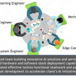
To cover all these bases, Bipin has built a team with a wide range of expertise:
- Machine learning – to define and drive neural network training and optimization for inferencing
- Sensor fusion – we casually throw this term around but making it work in a real application is still an art
- Embedded systems – for all aspects of the embedded software stack
- Edge architectures – for sensing and actuation along with reasonable power, communications and security
- Mechatronics – for the mechanical aspects of actuation
Bipin is very proud of this full-stack AI systems lab in the heart of Silicon Valley. He has deliberately chosen not to recruit seasoned veterans, even in these domains. Instead he staffs the lab with recent graduates, not locked into fixed ways of solving problems in this still-evolving domain. The lab in his view is his secret sauce, a unique way to architect and build out full-stack AI systems. And he walks this walk. When prospects or partners visit, they don’t get slideware, they get hands-on demos. Which of us wouldn’t take a working demo over death by PowerPoint? You can learn more about ICURO HERE.

