
Every system-on-chip (SoC) designer worries about power. Many widely used electronics applications run on batteries, including smartphones, tablets, autonomous vehicles, and many Internet-of-Things (IoT) devices. Even “big iron” products such as network switches and compute servers must be careful when it comes to power consumption. Not every customer can be located next to a hydroelectric dam or a power plant. Even those users willing to pay for vast amounts of electricity may have to comply with “green” laws that cap their draw on the grid.
In response to these requirements, the industry has developed a wide range of techniques to manage power consumption, from clever circuit designs to system-level software control. The most common approach is turning off portions of the SoC not currently active and then turning them back on when required. Instead of being completely powered on and off, the voltage and/or clock speed of a clock domain may be raised or lowered “on the fly” as needed to satisfy critical functionality and meet performance goals.
SoCs may contain dozens of clocks domains with thousands of possible off/on combinations, only some of which are legal. Power controllers that scale the domains up and down are very complex. It is a significant challenge for designers to understand the full scope of power management and for verification engineers to check all legitimate combinations. The consequences of a bug can be severe; a power domain that can’t be turned back on could lock up the chip. Even worse, too many domains powered on at the same time could lead to thermal runaway and chip failure.
So what is the poor SoC engineer to do? I recently talked with Cristian Amitroaie, the CEO of AMIQ EDA, about the power-domain visualization and navigation capabilities in their Design and Verification Tools (DVT) Eclipse Integrated Development Environment (IDE). It seems to me that their approach makes it much easier for design and verification engineers to create, manage, and validate power domains, from IP blocks all the way up to large SoCs. I’d like to review some of the features that struck me.
For a start, DVT Eclipse IDE handles both common formats for specification of power intent, including power domains. Common Power Format (CPF) came from The Silicon Integration Initiative (Si2), while Accellera defined Unified Power Format (UPF). UPF has been standardized as IEEE Std. 1801-2015, which was an attempt to merge the two formats. CPF advocates argue that the IEEE standard is missing some key features, but since AMIQ EDA supports both UPF/IEEE and CPF (version 2.0), SoC teams are free to choose their preferred format.
One critical feature in DVT Eclipse IDE is automatic generation of power supply diagrams from an IEEE Std. 1801 or CPF specification. These diagrams show all the power domains, the connections between them, and the signals from the RTL design that control the domains. Engineers can click on a power domain and jump to the location in the power-intent file specifying the details for the domain. Engineers can also click on a control signal in the diagram and jump to that same signal in the RTL source file. Thus, it is easy to cross-check the design and power-intent files.
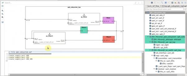
This ability is very useful since an IEEE Std. 1801 or CPF file is distinct from the RTL design files. This enables the separation of power intent from implementation, good practice when dealing with any sort of architectural specification. The downside is that it is common for the two descriptions to get out of synchronization as the design evolves. Renamed signals and changes in the design hierarchy can render the power intent file outdated. As Cristian points out, the visualization capabilities of DVT Eclipse IDE make it easy to keep track of changes.
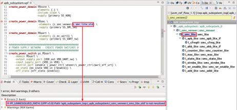
The IDE includes analysis engines “under the hood” that check for many types of problems. Any inconsistencies between the power-intent file and the design are detected and reported visually. DVT Eclipse IDE re-compiles its internal model whenever code changes are made, so it instantly cross-checks any edits to UPF/CPF or RTL files and reports any mismatches. The IDE also detects any syntax or format errors made in any of the design and verification files, including power intent.
In addition to the language and consistency checks, users specifying power domains can benefit from the same features available for all the other languages and formats supported by the IDE. Available features include the power supply network diagrams, source code editors, a hierarchy browser, and schematics of the design. It is easy to navigate among these screens while following a signal or an element in the hierarchy. Color coding is used to visually link common elements across multiple views.
If an engineer makes a mistake, for example typing “create_power_domains” into the UPF editor, the IDE instantly reports this as an error and recommends a correction to the proper “create_power_domain” command. The IDE also makes suggestions; typing in only “create_” pops up a menu showing the possible auto-completions and allowing the user to choose. The IDE can also generate a template for a new command, showing which fields the user must fill in, with both auto-completion options and error reporting available.
Cristian reports that their solution greatly reduces the time it takes to learn a standard and to create a power-intent specification, even for expert users who know the format well. The challenges of SoC power management continue to grow, and it’s hard to imagine designing or verifying a large chip without the support of DVT Eclipse IDE. More information is available, as is a short but impressive video. I encourage you to investigate further, absolutely.
To learn more, visithttps://dvteclipse.com/products/dvt-eclipse-ide.
Also Read
Renaming and Refactoring in HDL Code
I Thought that Lint Was a Solved Problem
Easing Your Way into Portable Stimulus
Share this post via:


Comments
There are no comments yet.
You must register or log in to view/post comments.