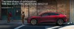
Bronco Webinar 800x100 1

Radio: Relevant, Unifying, Intimate, Vulnerable

Radio: Relevant, Unifying, Intimate, Vulnerable
by Roger C. Lanctot on 09-15-2019 at 10:00 am

It was hard to escape the notion while attending RadiodaysAsia2019  that the world is experiencing what can only be called “peak radio.” Radio has the widest audience reach of any content delivery medium anywhere in the world, with the possible exception of India, according to researchers such as Nielsen Media, Gfk, Rajar, Edison Research and others. And Radio is the most trusted medium, according to research from the European Broadcasting Union.

Digital radio (in the form of HD Radio, DAB and DAB+) is unfurling across Europe, North America and the rest of the world broadening and enriching the trove of content emanating from broadcasters around the world. The shift to digital is further transforming the medium adding visual elements and information services while enhancing the quality of the signals.

This increasingly digital and visual medium is also now searchable and manageable thanks to metadata which is being implemented station by station – while receivers are steadily being updated and upgraded. In fact, the Internet has allowed radio to reach into every nook and cranny of listeners’ lives  even as standalone radios have begun to disappear.

Radio Futurologist James Cridland, keynoting the event, noted further that radio creates communities and unifies listeners rather than dividing and inflaming audiences the way social media like Facebook, Twitter, and Youtube have perverted elections in the U.S., Europe, India and elsewhere. And, Cridland added, radio won’t violate your privacy.

Radio also won’t promote fake news. Researchers Lucile Stengel and Sapna Solanki of the BBC shared the results of a study published late last year on the impact of social media and fake news on elections in India. Suffice it to say, radio was not implicated.  The study can be found here: https://downloads.bbc.co.uk/mediacentre/duty-identity-credibility.pdf

Why, then, since radio appears to be riding a wave of media domination is there the eerie sense of competition closing in on the industry? It so happens that the Internet giveth and the Internet taketh away.

With the boost in audience reach that the Internet has enabled for radio (creating new ways to connect and interact with listeners) has come competition for the ears of listeners from music streaming services, podcasts, and Youtube. The latest rumor is that Facebook is poised to enter the streaming business as well.

The most feared competitive phalanx is FAANG – so-named by Julie Warner, Events Director for Commercial Radio Australia – Facebook, Apple, Amazon, Netflix, and Google. These organizations are targeting the ears, eyeballs, and wallets of radio listeners and putting pressure on broadcasters with billions of dollars in advertising at risk.

Nowhere is the onset of FAANG more notable than in the automobile, where as much as 50% of all radio listening or maybe more is occurring throughout the world. Amazon, Apple, and Google, in particular, are seeking to close the gap that the automobile creates in the otherwise comprehensive view they possess of consumer behavior in the form of search, transactions, and daily interactions.

The car is a browser on wheels operating largely off of the grid from normal search and information resources. The car is a hole in the broader search marketplace – worth $100B to Google. It is a vacuum and FAANG abhors this vacuum.

Car companies are seeking to capitalize on their privileged position as controllers of all that occurs in the car. The radio industry, too, is hoping to preserve its prime real estate perched in the center of the dashboard.

Toward that end Michael Hill, Managing Director of Radioplayer Worldwide UK spoke at RadiodaysAsia about the importance of adopting and deploying digital assets to enable rich in-vehicle digital experiences that are radio centric. In that vein, Radioplayer has introduced a reference design capable of integrating streaming services with terrestrial radio along with helpful visual elements designed to break radio out of the bonds of ancient “radio dial” interfaces into a more non-linear experience.

Companies like Zenon Media and Sheridan Broadcasting are taking radio further offering tools to integrate video content with radio’s audio content for both Internet-based delivery and in-vehicle rendering – perhaps in the frontseat? Anything is possible – especially now that Tesla Motors is tipping its intention to introduce Netflix and Youtube in dashboards.

The world is experiencing peak radio, as evidenced by research and insights shared at RadiodaysAsia2019. But preserving this leadership will take innovation and collaboration – particularly with the automotive industry. Unlike previous Radiodays events, RadiodaysAsia was missing a stronger representation of the automotive industry. Auto makers must tune in to the changes sweeping the broadcast industry.

Radio already delivers a location-relevant platform including news, weather, sports, traffic, and advertising with curation that creates an intimate experience for listeners throughout the world. The onus is on car makers to bring that experience to life in the latest digital dashboards. Today’s radio is digital, searchable, non-linear, intimate, community-creating, and personal. There’s nothing else quite like radio and it’s better than ever.


WEBINAR: Reusing Your IPs & PDKs Successfully With Cadence® Virtuoso®

WEBINAR: Reusing Your IPs & PDKs Successfully With Cadence® Virtuoso®
by Randy Smith on 09-13-2019 at 10:00 am

I recently wrote about a ClioSoft® study with Google on using cloud platforms for EDA design and the importance of using persistent storage when doing that. ClioSoft will again be sharing important information on design productivity in the upcoming webinar, Reusing Your IPs & PDKs Successfully With Cadence® Virtuoso®. SemiWiki will hold this webinar featuring ClioSoft on Tuesday, September 24, 2019, from 10:00 am to 10:45 am. You can reserve your space here with your work email address.

Over the past decade, the importance of design reuse has become not simply more important, but a mandatory requirement. You cannot design today’s chips, with their tremendous transistor counts, from scratch. There is not enough time. The lack of time to design from scratch is even more clear when we look at analog design. If you have a piece of analog functionality already working in a certain process, you should never redesign it without a very good reason; otherwise, you are simply wasting time and resources. It is not free to move analog IP between process nodes, but it is usually better than “reinventing the wheel.” So, if you are going to look for reusable IP inside your company, where do you start?

ClioSoft announced designHUB® in May 2017. It made its debut at DAC a month later. Since then, many companies have adopted designHUB to reuse their internal and licensed third-party IPs. With ClioSoft’s integration with so many EDA vendors, the adoption of designHUB has been increasing dramatically. This webinar will focus on using designHUB for analog design with Cadence’s Virtuoso.

Sourcing IP can be a time-consuming part of the design process. There is a point at which, if you have not selected the IP you are going to use for a specific function, the design process halts. When selecting IP, there are many things to consider:

  • Basic functionality – What does this IP do?
  • Specifications – In which process was it used? How fast is it? How big is it? How much power does it consume?
  • Features – Does this IP support all the features you need?
  • Usage – How often has it been used? In what types of designs?
  • Cost – Especially in the case of a previously licensed IP, it may not be free
  • Quality – You need to know the previous usage of the IP, and how well it has performed
  • Support – Is there an in-house expert who has used this product that can answer your questions? How do you learn about fixes and workarounds?

Managing and sharing all this information across your company is what designHUB provides. You enable your design community to crowdsource their IP using search mechanisms. You can also set up workflows for addressing the permissions necessary to utilize a given IP. Each design may now more easily share their IP with the rest of the company design community, improving design quality, and reducing design costs.

The webinar will be moderated by Dan Nenni,  Founder of SemiWiki. The presenter will be Karim Khalfan, Vice President of the Application Engineering group at ClioSoft. Karim has led the deployment of ClioSoft’s SOS7 design data and IP management across the semiconductor industry. He has written several articles and white papers on SoC design data management solutions. I have known Karim for more than a dozen years, and he is a friendly, funny, and smart person you will enjoy hearing him speak. Karim has received his Bachelor of Science degree in Computer Science from the University of Texas and holds a patent on defining a universal data management adapter to be used for integration with any EDA tool.

Be sure to sign up using your corporate email address now – here.

About ClioSoft Inc.

ClioSoft® is the pioneer and leading developer of enterprise system-on-chip (SoC) design configuration and IP-management solutions for the semiconductor industry. The company provides two unique platforms that enable SoC/IP design-management and reuse.

The SOS7 platform is the only design-management solution for multi-site design collaboration for all types of designs – analog, digital, RF and mixed-signal. The designHUB® platform provides a collaborative IP reuse ecosystem for enterprises.

ClioSoft customers include the top 20 semiconductor companies worldwide. The company is headquartered in Fremont, CA with sales offices and distributors in the United States, United Kingdom, Europe, Israel, India, China, Taiwan, South Korea and Japan. For more information visit www.cliosoft.com

Also Read

For EDA Users: The Cloud Should Not Be Just a Compute Farm

IP Provider Vidatronic Embraces the ClioSoft Design Management Platform

56thDAC ClioSoft Excitement


Chapter Ten – Design Automation for Systems

Chapter Ten – Design Automation for Systems
by Wally Rhines on 09-13-2019 at 6:00 am

Electronic design automation has evolved to an extent that the complex chips with tens of billions of transistors frequently produce first pass functional prototypes from the manufacturer.  What makes this so incredible is that such a small portion of the possible states of electronic operation are actually tested in the simulation of the chip.  Figure 1 takes the example of a very simple electronic function, a 32 bit comparator, that compares two thirty-two bit numbers and determines whether one of them is equal to, less than or greater than the other.  One might naively assume that this requires 2^32 comparisons of the two numbers.  It doesn’t.  If it did, then a caveman who was given one of today’s state of the art computer servers 565,000 years ago would just have completed the calculation.  EDA history is made up of innovations that preempt the need to check every possible state of an electronic circuit, or 100% of the state space as design practitioners would say.

Figure 1.  Simple comparison of two 32-bit numbers would require 565,000 years with a state-of-the-art computer if each possible pair of numbers had to be compared

The question then arises, “if we can reliably simulate the behavior of chips with billions of transistors, can we extend the technology to more complex systems like cars, planes and trains?”  Or, if we can do this for the electronic behavior of a chip, could we extend it to the mechanical, thermal, aerodynamic or other simulated behavior of a complex system? Inverse reasoning suggests that the answer is “yes”.  The reason is that the electronics of systems like cars and planes are becoming so complex that, if we can’t automate the design and simulation, there is no other known solution.  Humans certainly can’t analyze the complexity of such a system (Figure 2).

Figure 2.  Electronic and wiring complexity of a 2014 S-Class Mercedes

It has taken sixty years to evolve the software to accurately simulate the electrical behavior of chips.  How long will it be before we can do the same for an entire car or plane?  And how will cars and planes be designed in the meantime?

For the automotive and aerospace industries, mechanical design simulation and verification evolved long before electronic simulation.  Dozens of mechanical computer automated design, or CAD, companies emerged in the last thirty years. Today simulators that model most of the mechanical design, as well as the manufacturing processes to produce them, are available from companies like Siemens, Dassault and Parametric Technologies.  These simulators also analyze aerodynamics and thermal effects.

It’s just in the last three decades that the electronics in cars and planes have increased in complexity to such a level that humans can no longer manage the data required to create an optimized, cost effective design without errors (not to mention protections against hacking).

It’s easy to assume that the design of a car you buy has been verified by driving prototype cars for thousands of miles in all types of weather conditions.  It probably has.  Before a manufacturer can build that prototype, extensive verification must be performed.  How is that done?  It all comes down to a methodology called “abstraction”.  Requirements for the design of a vehicle are described at a high level and then refined to provide greater detail.  Each level of abstraction of the data is analyzed on a computer or with a physical prototype of a subsystem.

The same is true of integrated circuits.  Figure 3 shows the various abstractions used to describe, simulate and verify the performance of a chip.

Figure 3.  Four “abstractions” used in the design of integrated circuits

Although relatively new, ICs are increasingly being described in a high level language like C++.  This description is relatively compact so simulations of the entire chip, or the critical performance portions of it, can be run quickly.  That description is automatically “synthesized” into the next level of abstraction called “RTL” or register transfer logic that is described by a language such as Verilog, VHDL or System Verilog.  This level of abstraction is much more detailed, describing logical operations of the chip.  Simulations of the full chip typically take up to twenty-four hours so the building blocks of the chip are rigorously simulated before integrating them step by step until the whole chip that  can be simulated.  Once the designer is satisfied with the RTL simulation, the database is synthesized into a description of the actual logic gates creating what is called a “net list”.  The design is synthesized into a description of the physical layout of the transistor on the silicon and then transformed into a language (GDS2) that the photomask generator can understand and can convert into the actual photographic negative that is used to manufacture the chip.

System design has evolved a similar design approach but systems engineers refer to it as the “V Diagram” (Figure 4). A difference between the “V” approach and that used

Figure 4.  System “V” diagram showing the path from high level abstraction to greater detail followed by integration and verification at each level of abstraction

by IC designers is that the system designer is likely to build a physical prototype of each subsystem once the design is refined to the level of a physical description.  That prototype can then be tested by inserting it into a laboratory mockup of the entire vehicle using what is referred to as “hardware in the loop” testing. Integration testing can also be performed with hardware in the loop but increasingly those subsystems are tested in a “virtual” environment where the parts of the vehicle that are connected to it provide inputs and react to its outputs in a simulated virtual environment.

This whole methodology is being disrupted because of growing complexity.  Once we begin to develop truly autonomous vehicles, the approach will become totally inadequate because the number of tests that must be performed exceed the capability of physical testing (Figure 5).  To test an autonomous drive vehicle would require more than eight billion miles of driving, according to Akio Toyoda, CEO of Toyota.

Figure 5.  More than 8 billion miles of driving would be required to physically test an autonomous vehicle.  Instead “virtual” verification must be adopted

A manufacturer would have to send out a fleet of 300 cars, driving at 60 mph for fifty years.  Not very practical for introducing a new model each year.

Another reason that automotive and aerospace design must become virtual is that optimization has become too complex.  Consider the wiring alone.  With more than 1.5 miles of wiring in a car, forty miles in a small business jet and over one hundred in a commercial aircraft, there is a critical need to analyze tradeoffs among variables like weight, cost, performance, signal integrity, etc.  Finding an optimum combination is far beyond the ability of the human brain. The same can be said for optimizations of the electrical subsystems, called electronic control units or ECUs in a car, or line replaceable units or LRUs, in an airplane.  These ECUs contain multiple chips and embedded software to handle processing such as control of brakes, transmission or engine ignition.  They are complex enough to require simulation to assure that the inputs and outputs perform as specified.  The additional opportunities for problems arise when the ECUs are tested in a system environment.  Even if an automotive OEM were lucky enough to produce a functioning car without a virtual simulation, debug of future problems would be difficult or impossible without a simulation.

Modern cars contain up to one hundred million lines of software code.  It’s safe to assume that this code will contain bugs.  The challenge for the automotive OEM is to find a way to react quickly and update the software in every similar vehicle on the road when a bug is discovered.  Otherwise, the OEM could be liable for all accidents that occur once the bug is known.  Tesla has developed an infrastructure to make this possible.  The other challenge is to design the car in such a way that mission critical systems can be isolated.  Many of the most publicized hacks of vehicles have come from intrusion of the vehicle through the infotainment system that is tied to the CAN bus, giving access to more critical systems like the brakes, transmission and engine.

How long will it take until automotive OEMs design the entire vehicle, as well as the assembly line for building it, in a totally virtual environment on a computer.  The industry is farther along than you might think.  Most of the mechanical design and manufacturing operations are already done that way.  The remaining challenges include much of the electronics.  That’s why Siemens, who provided software for all aspects of mechanical, aerodynamic, thermal and manufacturing simulation, decided to acquire an EDA company, Mentor Graphics.

System simulation of the electronics, as well as testing and optimization that involves “cross domain” testing among electrical and mechanical systems, remains very challenging.  Wiring architectural tradeoffs and automatic generation of the design of the wire harness is essentially automated today.  Automation of design and verification of other vehicle electronics will require development of abstractions that can be used to analyze multiple ECUs operating in concert with one another as embedded software is executed in the vehicle.  The abstractions must be at a high enough level that they can be simulated at  something like 100X the real time execution but be detailed enough that an engineer can analyze the inner workings of an ECU to find a design bug or test an optimization alternative.

How long will this take?  Not that long.  It has to happen over the next decade or two or we won’t be able to design the next generation of cars and planes.


Synopsys is First IP Provider with a Complete CXL Implementation Available

Synopsys is First IP Provider with a Complete CXL Implementation Available
by Randy Smith on 09-11-2019 at 12:00 pm

Synopsys just announced the availability of their IP solution supporting CXL (Compute Express Link). This new protocol is going to be an important component for several applications expected to be shipping starting in 2021. CXL is an alternate protocol that runs on the same physical layer as PCI Express (PCIe). Among other usages, PCIe is the protocol running over the expansion slots on all PCs. Other standards have been written on top of the PCIe electrical interface including the laptop expansion card interface ‘ExpressCard’ and the serial computer storage interface SATA Express. In data centers, many applications have become based on special hardware plugged into PCs via the PCIe slots on the motherboards. Those specialized applications to some extent have been held back by the limitations in the PCIe protocol. CXL is the new standard to address the needs of these new applications while maintaining backward compatibility with PCIe.

We have all heard of the explosion in machine learning and artificial intelligence. These solutions are predominantly based on either GPU or FPGA accelerators. There will soon be an onslaught of cards with application-specific processors from any number of different processor architectures to support applications such as image, facial, encryption/decryption, various video processing functions, storage class memory, voice recognition, big data analytics, and other capabilities that all depend on a fast host connection while running in the PCIe slots. With so much intelligence available in the expansion cards, more was needed from the interface protocol – specifically the sharing of cache and memory data between the host processor and the accelerator card’s processors. CXL addresses this for several type of systems by supporting low latency and cache coherency.

The most significant feature of CXL is that it uses three unique protocols – CXL.io which is used for configuration and data management, CXL.cache which enables an attached device to cache data from the host’s memory, and CXL.mem which allows a host processor to access attached memory in a CXL device using standardized transactions. These protocols allow the attached accelerators to work more cleverly and efficiently with the host processor, and potentially through the host processor cache, with other attached accelerators. Keep in mind that PCIe is a point-to-point connection model, not a bus model. Each of the attached devices has a dedicated channel to the host. The host processor manages coherency of data cached by the attached devices.

So why do I think that this will be important in 2021? Easy, future Intel CPUs will support PCIe 5.0 and CXL, beginning in 2021. In March, we heard that “Intel sees CXL as being an alternate protocol running over the PCIe physical layer. At first, CXL will use 32Gbps PCIe Gen5 pipes, but Intel and the consortium plan to aggressively drive towards PCIe Gen6 (and theoretically beyond) to scale.” In July, AMD also signed on to CXL. While AMD is also in other potentially competing consortiums, Intel is only backing CXL for the protocol in this part of the computing architecture. There are also many other prominent companies backing this standard. By market strength alone, I would expect it to win, but beyond that, it seems like a very efficient approach as well.

Synopsys has announced a quite complete CXL solution. The DesignWare® Compute Express Link (CXL) IP solution consists of a controller, PHY, and verification IP. Synopsys’ CXL IP solution is compliant with the CXL 1.1 specification and supports all three CXL protocols (CXL.io, CXL.cache, CXL.mem) and device types to meet specific application requirements. And, of course, CXL IP is built on Synopsys’ DesignWare IP for PCI Express 5.0. Most importantly, you can license and start designing with this solution now for products shipping in 2021, when we expect Intel to be shipping systems supporting CXL as well.


Ford Prioritizes Safety; Revolutionizes Connectivity

Ford Prioritizes Safety; Revolutionizes Connectivity
by Roger C. Lanctot on 09-11-2019 at 10:00 am

Ford Motor Company’s debt may have been downgraded to junk this week, but the company’s savvy strategy for vehicle safety and connectivity has had an outsize influence on the broader automotive industry.  That is the takeaway message from this week’s ITS California gathering of transportation executives taking place in Los Angeles.

On the vehicle safety front Ford standardized a set of advanced driver assist systems (collectively known as ADAS) across much of its new vehicle line up with the goal of making these safety systems standard by 2020. The portfolio of safety features is collectively known as Co-Pilot360 and includes:

·       Automatic braking

·       Pedestrian detection

·       Lane keeping

·       Automatic high beams (car senses oncoming traffic and switches to regular beams to avoid blinding the other driver)

·       Blind-spot monitoring

·       Rear-cross-traffic alert

·       Backup camera

This move has set the stage for an enhanced insurance offering designed to use application program interfaces (APIs) to allow Ford vehicle owners to share vehicle data directly with insurance companies. To allow that data to be shared, Ford also announced its intention to connect all of its cars.

But the connections Ford intends to add are not just any connections. By 2022, Ford expects most of its cars to come with built in C-V2X technology – an LTE-based cellular system capable of allowing Ford vehicles to communicate directly with other so-equipped Ford’s or, indeed, any other vehicle with built in C-V2X modems.

Ford’s move contrasts with GM’s introduction of DSRC-based V2V technology on a single slow-selling Cadillac model; Toyota’s reversal of its announced plans to introduce DSRC in North America in 2021; and Volkswagen’s stated intention to fit all of its cars with DSRC. Ford’s C-V2X decision has set the company apart with a decision likely to bestow a leadership patina on the one-time connectivity laggard.

To emphasize the importance of this decision, Ford has been conducting technology demonstrations in Europe and the U.S. in partnership with Audi of America – demonstrating the ability of C-V2X connections to enable direct communications between vehicles from different manufacturers. This C-V2X deployment decision from Ford has fundamentally altered thinking in both the automotive and transportation industries around inter-vehicle communications and, in fact, vehicle-to-everything connections.

Ford, a founding member of CAMP (Crash Avoidance Metrics Partnership), operated under the aegis of the National Highway Traffic Safety Administration since 2001, has long advocated the use of DSRC-based 5.9GHz wireless spectrum for collision avoidance applications built upon vehicle-to-vehicle communications. Ford’s embrace of cellular technology for collision avoidance was a shock to both the automotive and the ITS communities.

ITS is short for Intelligent Transportation Systems. ITS California is the state chapter of the larger ITS America organization. Transportation and transit agency members gather annually to share information regarding new technologies and prioritize problem solving and spending.

The systems discussed, debated, and sold at ITS events such as the one held in Los Angeles this week are hardware and software solutions designed to leverage roadway cameras and sensors and wireless and wired connections to allow traffic managers to enhance vehicle throughputs on highways, bridges, tunnels, and city streets, reduce congestion and mitigate mishaps like vehicle crashes.

Prominent among the workhorse technologies for these organizations – including state-level departments of transportation and public transit authorities – is wireless technology operating in the 5.9GHz band. The 5.9GHz band has been assigned to transportation applications for more than 20 years, due in part to the work of CAMP. It is only recently that it has been aggressively employed for transit priority, traffic monitoring, congestion detection, traveler alerts, snow plow and emergency vehicle traffic signal pre-emption, and vehicle-to-vehicle collision avoidance applications.

Up until the end of the Obama administration much of the discussion around the use of the 5.9GHz band centered on so-called dedicated short range communications (DSRC) technology – a protocol designed to enable safety-relevant, low latency, inter-vehicle communications. The onset of LTE-based C-V2X and, soon, 5G wireless technologies – also operating in the 5.9GHz band – has changed the conversation.

Regulators in the E.U. and the U.S. are now reconsidering what was once expected to be a global technology mandate for DSRC adoption in passenger vehicles. The momentum toward a mandate stalled in the U.S. at the end of the Obama administration and received at least a temporary detour in the E.U. with the rejection of the DSRC-linked Delegated Act by member states this summer. China has simply rejected DSRC in favor of 5G and C-V2X cellular technology.

A subtle change in messaging from regulators and transportation executives in the U.S., though, reflects a sea change that has occurred in the industry thanks mainly to Ford’s decision to commit entirely to built-in C-V2X connections in cars. U.S. Secretary of Transportation Elaine Chao has consistently chosen language suggesting a technology agnostic stance for vehicle-to-vehicle communications – in itself a significant change from prior department messaging.

Chao’s messaging has now been picked up within the wider ITS community. When 50 U.S. state DOT’s sent a letter, in August, to the Federal Communications Commission insisting that the 5.9GHz be preserved solely for transportation applications, they did not specify or favor DSRC over cellular technology.

The FCC is testing the proposition that the 5.9GHz band might be shared with other unlicensed applications. The transportation industry is asking that the assignment of the spectrum for transportation be preserved (in the face of heavy lobbying from the cable industry), but has set aside its prior insistence on DSRC.

In reaction to Ford’s announcement of C-V2X deployment plans, DOT’s have begun to grasp the implications of cellular-based vehicle-to-everything communications. Most notable of all that C-V2X and 5G will enable is vehicle-to-pedestrian connections. It is widely, and finally, recognized that smartphones will never be equipped with DSRC. But some day most smartphones will operate on 5G networks.

The clincher at the ITS California event was the first offering of a dual mode (DSRC/C-V2X) roadside field monitoring unit from Applied Information. The automotive has seen dual mode devices from Continental and Bosch, but Applied Information is the first to offer this combination for infrastructure installations.

Applied has deployed C-V2X technology at hundreds of locations around the U.S., but the introduction of the dual mode device recognizes the reality that DSRC and C-V2X are likely to co-exist in the market – even if C-V2X has considerably greater momentum.

The arrival of the dual mode device, along with Applied Information’s broader offering of related C-V2X-based devices and systems, is a manifestation of the growing interest among state and city DOT’s in future-proofed, cellular-based systems. With Ford signaling its plans to fit C-V2X in ALL of its cars, the future of car connectivity and vehicle-to-everything connections is clear. A new era of vehicle connectivity and safety has dawned, ushered in by Ford.


Tcling Your Way to Low Power Verification

Tcling Your Way to Low Power Verification
by Bernard Murphy on 09-11-2019 at 5:00 am

OK – maybe that sounds a little weird, but it’s not a bad description of what Mentor suggests in a recent white-paper. There are at least three aspects to power verification – static verification of the UPF and the UPF against the RTL, formal verification of state transition logic, and dynamic verification of at least some critical inter-operations between the functional logic and power transitions such as correct req/ack handshaking with a turned-off function which must turn-on in order to acknowledge. This third set is where the white-paper introduces a Tcl-based methodology.

The author (Madhur Bhargava – lead MCS at Mentor) first contrasts the new approach with the traditional method to test compliance with any requirement in RTL verification – through adding SV assertions. He acknowledges that a number of verification tools provide support for power verification of this type, but points out that these come with several limitations:

    • Built-in checks don’t cover all the checks you will want to perform, so you’re going to have to complement these with some of your own checks
    • Adding your own checks is not so simple, particularly since you have to be very comfortably bilingual between UPF and SVA
    • And whatever checks you are performing, these runs will be slow because you’ve added a lot more checking overhead to your mission-mode functional checks.

The core idea behind the Mentor approach is to do power-verification checking post-simulation. Immediately you fix the third problem for regular verification regression users, though you still have to run your power checker. Next your power checker runs on the (post-simulation database. This uses a Tcl app based on the UPF 3.0 Information Model APIs, running on top of the waveform CLIs to access simulation data for use in Tcl-based procedures. That fixes the second problem – a power expert verifier no longer has to be multi-lingual; Tcl know-how (and UPF know-how) is all they need.

Finally you need to run your power checkers. These are going to check compliance with power intent by:

    • modeling control sequences/protocols
    • iterating over the design/power domains to access low-power objects
    • accessing the waveform info associated with these objects
    • checking for any mismatch with intent and flagging errors as needed

I find a number of things interesting about this approach. First this means that dynamic power verification doesn’t need to slow down functional debug and can run in a separate thread from that debug. This for me is another example of how elastic-compute concepts are becoming prominent in the EDA world.

Second, it’s good to see more open-minded approaches to verification. There’s a lot of good things in SV/SVA but we don’t have to be compulsive about dynamic verification only having to work through that channel. Exporting the data to Tcl-based apps for verifying power intent written in Tcl is a natural extension.

Madhur wraps up with some limitations to the approach. First the UPF 3.0 model has no concept of connectivity so checks requiring knowledge of source to sink paths (as one example) cannot be coded within the standard. I think this is purely a standards issue; providing a Tcl API to design connectivity is a problem that has been solved a long time ago. The committee just needs to find a mutually agreeable way to incorporate appropriate APIs.

He also mentions that an SVA assertion can abort a simulation run as soon as an error is found whereas this approach, being post-sim-based, will not trigger an abort. I think this a minor consideration. If simulation regressions are also going for functional verification, that’s not necessarily a bad thing – much of the simulation may still be useful after that event. Power intent debug continues on a parallel path and power bugs can be fed back and rolled up with all other issues, as discovered.

You can read the white paper by registering HERE.


GM’s Dashboard Surrender

GM’s Dashboard Surrender
by Roger C. Lanctot on 09-10-2019 at 10:00 am

There was a time when General Motors’ OnStar offering was readily and clearly understood by consumers for the fact that it did one thing incredibly well: summoning assistance in the event of a vehicle crash and airbag deployment. This now-23-year-old connected car solution still stands strong as a powerful brand-defining statement in the midst of an industry-wide muddle over what a connected car is and does.

Sadly, in recent years, GM has become fixated on “monetizing” vehicle connectivity – mining the vehicle connection for value propositions related to contextual marketing and subscription-based services. In the process, the OnStar brand has been muscled aside by competing value propositions ranging from Maven (mobility) to Marketplace (contextual marketing), MyLink (in-dash apps and smartphone projection), and embedded Wi-Fi from AT&T.

Recently, GM cut back the OnStar free trial to one month and terminated the personal minutes that allowed consumers to make phone calls directly over their embedded OnStar connection – not for free, of course. Interestingly, OnStar is zigging here (cutting the length of the free trial period) while the rest of the industry (VW and others) are expanding free trials from months to years. The cutback of personal minutes, while logical in the context of Bluetooth-connected smartphones removes one of the charming novelties of the OnStar solution – and what once represented the first hands-free in-car phone solution.

Most recently GM has offered unlimited data to select Cadillac owners for $15/month, throwing in three months of free access to Pandora Premium as a deal sweetener. This offer shows GM desperate to monetize the Wi-Fi capability of its OnStar embedded solution – ignoring the reality that most Cadillac owners likely have Wi-Fi access via their smartphones and won’t need or be interested in such an offer.

This offer is particularly ironic in the context of the personal minutes termination. It makes sense to end personal minutes given the availability of Bluetooth smartphone connections. By the same token, pushing Wi-Fi from the device built into the car (when Wi-Fi is already built into most smartphones) makes little or no sense – regardless of whether three free months of Pandora Premium are thrown into the offer.

The reality is that the Cadillac offer of three free months of Pandora actually looks pusillanimous relative to Porsche’s offer of three years’ worth of free streaming of Apple Music in the new Taycan. The bottom line is that GM is muddying up the value proposition of the OnStar brand with meaningless adjustments and penny ante offers that don’t speak to the core value proposition of the platform.

OnStar has always been about safety. At a time in the market when insurance companies and Tier 1 suppliers and even highway infrastructure companies are all looking for ways to reduce highway fatalities and reduce collisions by leveraging vehicle connectivity, GM’s OnStar has shifted its focus to streaming apps, Wi-Fi, and in-vehicle advertising and vehicle-based commerce.

Just in the past two weeks news has arrived of GM adding SiriusXM’s 360L in-dash interface and, as of yesterday, upcoming plans to deploy the Google Automotive Services platform. These systems will join the existing in-vehicle integration of Apple CarPlay, Android Auto, and GM’s own MyLink smartphone-based app platform – plus Xevo’s Marketplace.

All of this means the integration of multiple voice interfaces, multiple payment platforms (Xevo plus SiriusXM), a half dozen or more user interfaces, multiple navigation options, a half dozen traffic information sources (at least two options available within SiriusXM alone), and a data exchange free-for-all magnified by GM’s separate $25M investment in Wejo – which has begun acting as a GM connected car data broker. Completely absent from this moshpit of dashboard integrations is a consistent vision of customer engagement and retention with an emphasis on vehicle care and safety-prioritized operation.

Companies such as BMW and Daimler are already several years into vehicle integration programs that enable car-to-cloud-to-car communications of road hazards. Audi and BMW have been pioneering the integration of cellular-based traffic light signal phase and timing communications.  Audi has even added automatic toll-payment integration. Ford, Volvo, Daimler and BMW have joined the European Union’s Data Task Force for integrating vehicle-based data with infrastructure-based data sources to communicate traffic alerts and road hazards – all in the interest of reducing crashes and highway fatalties.

The one place in the car where car companies have the opportunity to interact with consumers and define their brand values and value propositions is in the center-stack display (and maybe in the instrument cluster). While Volvo, Ford, Daimler, BMW, and Audi are staking their claim to safety leadership, GM is capitulating to commercial priorities and seeking to drive in-dash commerce and peddle vehicle data.

This embarrassing lack of strategy and vision marks GM’s complete abdication of its once-vaunted safety leadership. While Ford Motor Company is standardizing advanced driver assist features and opening up vehicle APIs for insurers to offer discounted coverage based on vehicle operation, GM remains a laggard in deploying ADAS tech and a leader in in-vehicle driver distraction.

It’s not really a surprise given that most of the original OnStar team has now either retired, been bought out, or moved on. The DNA of the team that brought the groundbreaking OnStar system – Project Beacon – to the market more than two decades ago is long gone. The division has been renamed Global Connected Consumer Experience. The mission is now an incomprehensible muddle.

A group that once controlled its own hardware and software development – its own destiny – has been gutted. The leadership has been told to fend for itself by generating revenue from a platform that was conceived to assist drivers in need of assistance after catastrophic crashes – not for delivering in-dash coupons.

GM has surrendered its dashboards. This is the saddest turn of all. A leader has become a laggard in pursuit of what the company perceives as the next great challenge. But the original value proposition remains. With 100 people dying on U.S. highways every day and with 1.2M million humans dying on roadways globally every year the priority must be: saving lives, and avoiding crashes.


AI Chip Prototyping Plan

AI Chip Prototyping Plan
by Daniel Nenni on 09-10-2019 at 6:00 am

I recently had the opportunity to sit down with a chip designer for an AI start-up to talk about using FPGA prototyping as part of a complex silicon verification strategy. Like countless other chip designers for whom simulation alone simply does not provide sufficient verification coverage, this AI start-up also believed that FPGA prototyping would be a critical part of a successful chip delivery plan. When millions of dollars are at stake for advanced silicon geometry masks, not to mention the potentially fatal consequences of a startup missing a market window, getting silicon right the first time is key to success. This AI chip designer was running into FPGA prototype platform capacity limitations … and running out of time.

Learn about AI prototyping by attending this webinar replay: How ASIC/SoC Prototyping Solutions Can Help You!  Register now! Complex SoC case study included!

Throughout our discussions I couldn’t help being reminded of the value of a well thought out FPGA prototyping Plan early in the chip development process to minimize nasty surprises late in the design cycle. Considerations like: what chip functionality needed to be prototyped and when, estimated FPGA gate capacities, what prototype performance would be needed, how the prototype would be tested, etc. In addition, FPGA prototypers should consider how could the FPGA prototype will be easily scaled from one phase of prototyping to the next.

We reviewed the AI chip designer’s FPGA prototyping “vision”, and what options were available to complete the FPGA-based verification, and then scale up for customer demonstration platforms and more comprehensive design verification. The conversation revealed that there were three phases envisioned for FPGA prototyping;

· Phase 1 – verification of a “minimum slice” of the AI chip including a few AI processor cores before tapeout

· Phase 2 – an FPGA platform for a “larger slice” of the AI chip including more AI processor cores for early customer demonstrations, preferably before tapeout to assure alignment with customer needs

· Phase 3 – at some later stage, an FPGA prototype of the whole AI chip, where the whole AI chip would require about one billion equivalent ASIC gates from the FPGA prototype! Yes, that’s billion with a “B”.

Phase 1 was the immediate concern for this AI project, and a solution was needed quickly to allow enough time for good AI chip test coverage before tapeout. With minimum resources, start-ups do not have the luxury of major late-stage corrections to any part of their verification strategy, so changing FPGAs to get more gate capacity would require some trade-offs; do less with the available FPGA platform, or change to a bigger FPGA and run the risk of impacting tapeout schedules. FPGA gate capacity scaling can be accomplished by changing to a larger FPGA, or by using multiple FPGAs with the inherent need to partition the design between the multiple FPGAs … each approach has its pluses and minuses when it comes to impacting project effort.

Phase 2 should be scalable from Phase 1, if the Phase 1 FPGA platform provides a smooth path to scale up gate capacity for Phase 2. If Phase 2 calls for multiple FPGAs, and the Phase 2 approach is a linear scale up from Phase 1, which is usually the case with AI chips composed of a large array of identical processors, the choices made for the Phase 1 platform can simplify the Phase 2 solution.

Phase 3, at a billion gates, requires a separate discussion, and traditional emulation is the easy answer. The challenges with emulation are cost and performance. This AI company has considered emulation but found it simply too expense for a start-up. The company thinks it has the technical expertise to build a billion-gate FPGA prototype but has the good sense to admit that such an undertaking would be monumental and not the primary focus of their business. And then there is emulation performance, which sacrifices performance for high design visibility. While an emulator can achieve performances of close to 1MHz, FPGA prototypes are capable of performances of tens of MHz.

S2C’s Prodigy Family of FPGA prototyping solutions provide ample FPGA gate capacity options using either Intel FPGAs or Xilinx FPGAs … the user may choose their favorite brand of FPGA, a decision which is usually based on design tool preferences. The largest Xilinx FPGA is the VU440, which will support 30M to 40M effective logic gates, assuming a conservative gate utilization of 50% to 60%. Prodigy Logic Modules come with one (Single), two (Dual), or four (Quad) VU440 FPGAs, which translates conservatively to a range of available gate capacities from about 30M gates to over 100M gates.

The Prodigy Family also offers a high speed channel for the transfer of large amounts of transaction-level data between the FPGA prototype and a host computer (ProtoBridge), multi-FPGA debugging that allows deep off-chip trace storage (8GB), multi-FPGA trace viewing in a single window (MDM), and a rich family of ready-made daughter cards (80+) for quick assembly of a prototyping context.

S2C has been in the FPGA prototyping business for over 15 years, so their prototyping hardware is solid. S2C pricing for the VU440 Logic Modules starts at under $50K for a Single Logic Module and scales up to the Quad Logic Module. To get a quick S2C quote click here.

Learn about AI prototyping by attending this webinar replay: How ASIC/SoC Prototyping Solutions Can Help You! . Register now! Complex SoC case study included!

Also Read:

WEBNAR: How ASIC/SoC Rapid Prototyping Solutions Can Help You!

Are the 100 Most Promising AI Start-ups Prototyping?

FPGA Prototyping for AI Product Development


For EDA Users: The Cloud Should Not Be Just a Compute Farm

For EDA Users: The Cloud Should Not Be Just a Compute Farm
by Randy Smith on 09-09-2019 at 10:00 am

When EDA users first started considering using cloud services from Google, Amazon, Microsoft, and others, their initial focus was getting access for specific design functions, such as long logic or circuit simulation runs or long DRC runs, not necessarily for their entire design flow. If you choose to use the cloud this way, you allocate virtual machines, and all the files related to the job are uploaded. Once the results are transmitted back to the user, you release the virtual machines, including their associated storage. While this sounds simple, it is likely very inefficient to keep uploading many of the same files with each job. We need to consider persistent storage in the cloud to see how it competes with on-premise design centers.

WEBINAR: Reusing Your IPs & PDKs Successfully With Cadence® Virtuoso®

Rather than looking to the cloud services as a one-off compared to your internal computing center(s), consider it yet another compute center. Users of ClioSoft’s SOS7 design management platform already have been efficiently managing the shared data between different worksites with great results. Frequently used data is cached locally for greater efficiency. It is also seamlessly managed by SOS7 along with revision control and all the other aspects of design data management. The main ingredient to add to your cloud solution to make this work is persistent storage, such as Google Cloud Filestore (GCF). Recently, ClioSoft worked with Google to obtain hard data to quantify the benefits of this approach.

Setting up the environment was straight forward as ClioSoft documented on Google Cloud Blog site.  ClioSoft than ran through some of its standard benchmarks that simulate typical EDA customer workflows. Some comparative environments were also set up to measure the differences in performance. The results were quite informative and contained some surprises.

Perhaps the first takeaway is that setting up a design center environment in the cloud is not significantly more difficult than setting up an on-premise design environment. Users now need to consider the cost of maintaining their on-premise design centers as opposed to building their design environment n the cloud. Certainly, costs will be shifted from capital expenses to operating expenses. I will leave that to the CFOs to study further.

Focusing on just the file system interactions is important here as obviously performance gains can come from faster CPUs, as well. In general, the simulations show that SOS7 performance on GCP is as good or better as compared to on-premise systems. When an on-premises network uses shared NFS/NAS storage, performance was measured to degrade by taking nearly three times as long. A most notable discovery was that Cloud Filestore provides a near-local drive performance level while providing all the benefits of a shared drive.

Worst case, I think these results show that you will not lose any performance by using cloud computing with persistent storage, at least not with GCP and Google Filestore. I should note that Google also just announced the acquisition of Elastifile. Google describes Elastifile as a pioneer in solving the challenges associated with file storage for enterprise-grade applications running at scale in the cloud. They’ve built a unique software-defined approach to managed Network Attached Storage (NAS), enabling organizations to scale performance or capacity without cumbersome overhead. Google is expected to integrate Elastifile with Google Cloud Filestore following the completion of the merger.

Cloud performance aside, I am anxious to see how the larger EDA companies will evolve their business models to handle the increased usage of the cloud. This issue was a significant point raised by Joe Costello at Semicon West in July (more details in my blog on that topic). Users are likely to want to pay for EDA tools only when they use them, as you would expect with a SaaS model. Hopefully we will have more to share about that topic soon as well.

The usage of the cloud is only going to increase for EDA designers. Thanks to ClioSoft for analyzing the different ways to use the cloud and showing the huge benefit of using persistent storage in the cloud.

WEBINAR: Reusing Your IPs & PDKs Successfully With Cadence® Virtuoso®

Also Read

IP Provider Vidatronic Embraces the ClioSoft Design Management Platform

56thDAC ClioSoft Excitement

A Brief History of IP Management


Actel TI and TSMC Foundry Woes

Actel TI and TSMC Foundry Woes
by John East on 09-09-2019 at 6:00 am

TSMC was founded in 1987 by Morris Chang.  At about the same time, I was wrestling with the question of whether or not to join Actel.  Morris had been a top executive at Texas Instruments during the period when TI took ownership of the TTL market.  (See my week #8.  Texas Instruments and the TTL Wars)  I have to admit that when I first heard about what TSMC was doing I was unimpressed.  I didn’t like their prospects at all.  (I was wrong.)  I was a VP at AMD then. TSMC was anxious to do business with AMD.  After having a few discussions with Steve Pletcher, their VP of sales at the time, I formed the opinion that TSMC was ready, willing, and able to do business with pretty much anyone who came to them.  (Wrong again!!)  Besides TSMC, there was also a lot of foundry capacity available in Japan.  Most of the Japanese DRAM manufacturers had overbuilt their fab capacity during the boom of ’83 / ’84 and were willing to act as foundry sources for American IC houses. So  — my analysis was — there’s plenty of capacity available to fabless semiconductor companies.  If I join Actel, foundry will be the least of my worries. (Wrong again.  Three strikes and you’re out!!!)

There was a problem.  There were indeed many different companies with fab capacity. Yes.  They were willing to take foundry business.  But!!! Essentially none of them were interested in doing business with a custom process.  They all had standard processes and wanted to sell those wafers —– They didn’t want to spend money developing new processes – especially processes that would be used by just one customer.   To exacerbate the problem, I hadn’t analyzed the process requirements well enough when I was deciding to join Actel.  The process we needed was difficult!  Really,  really difficult!!!  Several new steps were going to be problematic, but one of them  — a requirement to build a very, very thin ONO layer with extremely tight control  — was nearly a killer.  No one wanted that headache in their fab.  To boot, my arguments to the foundries about the huge volumes that we would soon be ordering fell on deaf ears.  They just weren’t buying it.  Despite numerous requests,  TSMC always declined our business, politely telling us that they’d be happy to make wafers for us using any standard process they had.

When I arrived at Actel, we had one firmly established foundry relationship  —  Data General.  DG was a Boston based minicomputer company who had a small, old fab in Sunnyvale.  It was OK for proving out our product,  but it wasn’t at all a modern,  low defect fab.  Our yields would be low and our costs high if they were to be our primary foundry.  It didn’t look like it would be a good long-term relationship for Actel.  I wondered what to do about that.  While I was wondering what to do about it, they solved the problem for me.  They announced that they were shutting down the fab immediately leaving us fabless in the true sense of the word!  To be a fabless company with a complex,  non-standard process that no foundry wants to run is not a good thing!!   ☹☹☹

We had been having discussions with Matsushita Electric Corporation.  (MEC)   They liked the idea of programmable products in general and reasoned that it might be good to have access to our technology.  They had already made a few test runs of wafers in their R&D fab for us by the time I got there.  Their idea was to get a handle on just how hard the process would be to run.  In fact, they had many problems,  but at least the yields weren’t zero. Of course, we didn’t want to give them rights to sell their own FPGAs, but were willing to give them rights to use our technology in their ASICs.  After almost a (very worrisome) year of negotiating and tinkering around in their R&D fab, they agreed to bring up our process in their production fab if we would let them be our sales rep in Japan.  We agreed.

All of that sounded good except that the market for ICs was picking up. MEC’s fabs were filling up.  They had no appetite for spending a lot of effort on our custom process when they had more business than they could handle with their own products and processes.  In the end they did bring up our process. A lot of problems had to be solved along the way,  but they brought it up.  We owe them a lot!  But the rules were pretty simple.  Don’t jerk them around!!!  Requests for process tweaks, line holds,  splits etc would not be tolerated!  Those were tough rules that would affect us greatly in the days to come, because our process was far from stable — it needed a lot of work!  There seemed to be a new process problem lurking behind every bush  — and there were lots of bushes!!!

Parallel to the MEC negotiations,  Actel had also begun negotiations with TI.  The general idea was TI was going to give us some cash and guarantee us foundry capacity.  In return they would get second source rights to the first two Actel families.  The negotiations progressed well for a while,  but then reached an impasse.  By the time I came on board,  negotiations had ceased.  Both sides had walked away from the table. The deal was dead. I joined Actel the morning of December 1,  1988.  Early that afternoon Bill Davidow (Who was on our board.) called me and told me that I needed to go to Texas and patch things up in a hurry.  He was understating it.

So  –  the December 1988 status was this:  TSMC had turned us down. Data General was shutting down. TI was dead, and MEC was not looking good.   We were in trouble!!  We had a mask set and nowhere to run it. Cash was beginning to run low.  We needed to begin work on another round of venture financing,  but I couldn’t imagine anyone giving us money if we didn’t have a fab committed to building our product. A quick but easy to understand summary?

 Looks like we’re screwed!!

I wondered if AMD would take me back.

Happily, TI was willing to restart the talks. I flew to Texas with my fingers crossed.  Wally Rhines was to be the guy on the other side of the negotiating table.  Wally ran the integrated circuit business for TI.  I didn’t know Wally,  but I knew several high-level TI execs by reputation.  Maybe if Wally does another series for Semiwiki he can elaborate,  but the short version  — they were very, very, very tough people.  Fred Bucy?!!  Mark Shepherd?!! Morris Chang?!!  Wow.  You didn’t want to mess with them!!  So,  my mental picture of Wally was a huge man with glowing red eyes, horns, and a tail.  When I flew to Dallas for our meeting, I didn’t plan on liking Wally.  I figured that I was in for a tough day!

To my surprise, Wally turned out to be just the opposite.  Very bright, but also logical,  sensible, and reasonable.  After trading a few pleasantries, it might have taken us an hour or so to get things settled.  They agreed to be a foundry for us.  It took about two years to get the contract drafted and then the process working right, but once we did, they did a good job for us. What a relief.  Thanks, Wally!

But,  while I’m at it,  a little more about Wally Rhines.

In those days, it seemed as though everywhere I went, I ran into Wally talking about digital signal processing (DSP).  Technical conferences.  Wall Street conferences. Instat.  Everywhere!  Wherever I went, there was Wally making presentations about DSP.  To be honest with you, I had only a vague idea of what DSP was and really no idea at all of what it was good for.  To me it looked just like any other microprocessor except that it had an on-board hardware multiplier.  “So what?”  I thought.  The application example he always used was to calculate the five day running average of the Dow-Jones.  Again,  “So what?”

The fact was that TI had missed the boat in microprocessors.  In fact, everybody but Intel and AMD had missed that boat, but it took some companies a long, long time to figure out that they had missed it.  Everybody knew that microprocessors were going to be super important.  My sense was that Wally was only trying to assuage his conscience for that miss by talking about some hypothetical but unlikely upcoming DSP surge that TI would own.  I was wrong. He was right.  He was onto something that it took most of us a long time to figure out.  DSP was the missing link when it came to merging the real world (Analog) with Moore’s Law.

Today DSP is at the heart of all electronic communications  — there’s a huge amount of signal processing done in every cell phone and in all the communications links that exist.  At the end of the day, DSP was what allowed TI to become a 100 billion dollar market cap company. Congrats Wally.  Hope you were on commission!!  Wally later left TI to become CEO of Mentor.

MEC came up to speed and did a nice job for us for 25 years.  TI came up to speed as well and did foundry for us until we bought out their FPGA business in 1995.  In both cases, though, the process was a generation or two behind the state of the art. Xilinx products were always made on state of the art processes.  That was a very serious problem!!!

Next week:  More foundry woes.  How to get access to a state of the art process?

Pictured:  Wally Rhines.

See the entire John East series HERE.

# Bill Davidow, Fred Bucy,  Mark Shepherd, Morris Chang, Wally Rhines, DSP, Matsushita