Three years ago my youngest son purchased a $17 smart watch on eBay, but then my oldest son read an article warning about how that watch would sync with your phone, then send all of your contact info to an address in China. My youngest son then wisely turned the watch off, and never used it again. Hackers have been able to spoof and hide obstacles from the Tesla Model S using Autopilot. In 2015 hackers took control of a Jeep Cherokee through its entertainment system. A researcher in 2016 showed how he could control his or any other Nissan Leaf over the Internet.
Clearly we live in a connected world and the number of security threats to life-critical areas need to be contained. The experts at Methodics just conducted a webinar on this topic: IP Security Threats in Your SoC, so I watched the 25 minute archived video to find out if there’s hope against security breaches .
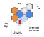
Vishal Moondhra was the presenter and he noted how semiconductor IP use is growing, with a single SoC often containing 100’s of IP blocks. The most sensitive electronic design areas are considered life-critical: automotive, medical, aerospace and industrial.
IP use is really quite a patchwork, with blocks coming from multiple sources:
The entire process of creating an IP block is quite dynamic, taking months to years with many versions being released along the lifecycle in order to meet changing requirements. IP users often have many tough questions which impact security, like:
- Which version of each IP is really being used?
- What scenarios for attack have each IP been subjected to?
- Are there security vulnerabilities in each IP being used within an SoC?
Let’s consider the example of a USB core, where during post-silicon penetration testing a security issue is uncovered. Which USB core version was being used? Who provided the IP? Did previous versions have the same security issue? Are there other cores using the same IP?
Answers to these questions often take too much time, they could be incomplete, and they requires collaboration between multiple engineers across teams probably using spreadsheets and documents. This is not a good security approach.
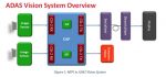
There is a systematic way to meet these security challenges by using enterprise traceability with an IP Lifecycle Management approach in the Percipient tool from Methodics. Here’s the big picture of how Percipient fits into an ecosystem:
Starting at the bottom we see the Data Management (DM) layer which uses industry standard DM tools. On top of that is workspace management layer where each engineer has their specific portion of an SoC design. The IP Lifecycle Management (IPLM) layer is where engineers control the release management process. At the meta-layer there’s information attached to each IP block like which engineers are using it on projects and any special IP properties. The Bill Of Materials (BOM) layer is fully addressable, so you know exactly what your SoC project really contains, in a full hierarchical fashion.
In this too flow there are multiple vendor tools integrated like Jira for bug reporting, Jama and Doors for requirements gathering, even simulators from EDA vendors. The analytics portion allows you to quickly find out about any project, and know the overall security vulnerability of your system
The standards body Accellera has an IP Security Assurance (IPSA) Working Group, and Methodics is a member of that, because it takes a village to ensure that IP security is done right.
With a tool like Percipient you can now easily track the consumption of all IP use, like: who is using an IP block, where each IP block is being used, versions of an IP, report bugs per IP, even check IP against a list of approved projects. Once this is all setup, you can measure the security level by looking at a dashboard or traversing the IP hierarchy fo security issues where the colors define the security severity:
For IP BOM management there are three main features provided:
- IP traceability
- Versioning with dependencies
- SoC version history
With Percipient there is traceability for all of the IP blocks and each workspace being used per engineer on the project, which enables the system to identify which users are affected by any IP version change. Event notifications are then automated for each engineer involved, so there are no costly communication delays.
The BOM is traceable and integrated with Jira for bug tracking, so all security impacted IPs are revealed. This traceability is created by adding a ‘security concern’ field for each bug, then Percipient rolls up all of the security concerns, and the displays the known Security Threats.
A live demo was then performed, walking us through how to use both Percipient and Jira tools to report bugs, assign security issues to an IP block, then seeing how the security matrix is auto-updated with the latest issues.
The final webinar part had Mr. Moondhra answering questions that were asked by attending engineers.
Q&A Session
Q: In the dashboard of security numbers, where do they come from?
A: All of the security numbers are automatically rolled up from the entire IP hierarchy of an SoC. In our demo, we had 28 concerns, 4 high, 1 medium, and 23 low. This live number is auto-updated as time progresses, and the integration ensures consistency between Jira and Percipient.
Q: How easy is it to bring 3rd party IP into Percipient?
A: We’ve made it easy to import IP, so each new IP version is typically brought in as a tar file using check-in with a tool like Perforce, then you release a new version into Percipient, and it takes just seconds,
Q: Who fills out security concern field?
A: The users who track bugs and security issues, using the Jira tool.
Summary
The challenges of IP security threats are a real and growing concern for teams building new SoCs. Using tools like Percipient and Jira for safety-critical designs in automotive, medical and other human-life fields makes a lot of sense. Instead of trying to create your own home-grown software patchwork, why not give Methodics a call to see how their approach would fit into your methodology.
Watch the archived video here.
Related Blogs