The concept of applying useful clock skew to the design of synchronous systems is not new. To date, the application of this design technique has been somewhat limited, as the related methodologies have been rather ad hoc, to be discussed shortly. More recently, the ability to leverage useful skew has seen a major improvement, and is now an integral part of production design flows. This article will briefly review the concept of useful skew, its prior implementation methods, and a significant enhancement in the overall design optimization methodology.
What is useful skew?
The design of a synchronous digital system requires the distribution of a (fundamental) clock signal to state elements within the digital network. A specific machine state is “captured” by an edge of this clock signal at state element inputs. Concurrently, the transition to the next machine state is “launched” by a change in the state values through fanout logic paths, to be captured at the next clock edge. The collection of logic and state elements controlled by this signal is denoted as a clock domain, which may encompass multiple block designs in the overall SoC hierarchy.
Current SoC designs incorporate many separate clock domains associated with unrelated clocks. The signal interface between domains is thus asynchronous, requiring specific logic circuitry (and electrical analysis) to evaluate the risk of anomalous metastable network behavior. (Clock domain crossing analysis, or CDC, is applied to the network to ensure the metastable design requirements are observed.)
The subsequent discussion will utilize the simplest of examples – i.e., a single clock frequency with a common capture edge to all state elements, and a clock edge-based launch time. Advanced SoCs would often include domain designs with: both rising and falling clock edge-sensitive state elements (with half-cycle timing paths); reduced clock frequencies by dividing the fundamental clock signal; and, latch-based synchronous timing where the launch time could be a state element data input transition while the latch clock is transparent. This discussion does not address clocking considerations common in serial interface communications, unique cases of asynchronous domains with “closely related” clocks – e.g., mesochronous, plesiochronous domains. This discussion also assumes the clock domain is isochronous, although there may be instantaneous deviations in the clock period at any state element input due to jitter – in other words, there is a single fundamental clock frequency throughout the domain over time.
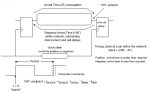
The figure below is the typical timing representation used for a synchronous system. A clock distribution network is provided on-chip from the clock source (e.g., an external source, an on-chip PLL), through interconnects and buffering circuitry to state elements.
The figure also includes a definition of the late mode timing slack, measured as the difference between the required arrival time and the actual logic path propagation arrival time.
The interconnects present from the clock source and between buffers could consist of a variety of physical topologies – e.g., a (top-level metal) grid, a balanced H-tree, a spine plus balanced branches (aka, a fishbone). The buffers could be logically inverting or non-inverting signal drivers or simple gating logic with additional enable inputs to suspend the clock propagation for one or more cycles.
The time interval between the clock launch edge and subsequent (next cycle) capture edge is based on the fundamental clock period, adjusted by two factors – jitter and skew.
The jitter represents the cycle-specific variation in the clock period. It originates from the time-variant conditions at the clock source, such as dynamic voltage and temperature at the PLL circuitry and/or thermal and mechanical noise from the reference crystal.
The skew in the arrival of the launch (cycle n) and capture (cycle n+1) clock edges also defines the time interval for the allowable path delays in the logic network. The skew is due to a combination of dynamic and static factors. Dynamic factors include: voltage and temperature variations in clock buffer circuitry, temperature variations in interconnects, capacitive coupling noise in interconnects. The static factors include process variation in the buffer circuits and interconnects, plus physical implementation design differences between the clock endpoints. More precisely, the skew is the difference in clock edge arrival at the two endpoints due to factors past the shared clock distribution to the endpoints, removing the common path from the source.
The time interval for logic path evaluation is the clock period adjusted by the design margins for jitter and (static and dynamic) arrival skew. From the launching clock edge through the state elements and logic circuit delays, the longest path needs to complete its evaluation prior to the capture edge, accounting for the jitter plus skew margins and the setup data-to-clock constraint of the capture state element.
To accommodate a long timing path, one of the potential optimization solutions would be to intentionally extend the static skew to the capture state element(s) through the physical implementation of the buffer and interconnect distribution differences between launch and capture. Correspondingly, the time interval for logic path evaluation from the delayed clock to its capture endpoints is reduced. This is the foundation of applying useful skew.
Traditional Methods
The conventional methodology for timing closure utilizes distinct tools for logic synthesis, construction of the clock physical distribution, and cell netlist placement and routing (adhering to any existing clock implementations). For synthesis, a set of clock constraints are defined – e.g., period, jitter, max skew implementation targets, distribution latency target from the block clock input to state endpoints. These targets were applied uniformly throughout the synthesis model (i.e., no arrival skew variation). Long timing paths were presented to various optimization algorithms focused on logic netlist and interconnect updates – e.g., higher drive strength cell swaps, signal fanout repowering buffer topologies, place-and-route directives to preferentially use metal layers with lower R*C characteristics. The figure below illustrates some of the potential repowering strategies employed during synthesis.
For state element hold time clock-to-data transition timing tests, the skew target was added to the same clock edge between short launch and capture paths, to ensure sufficient logic path delays and stability of the data input capture. Algorithms to judiciously add delay padding to short paths not meeting the skew plus hold-time constraint would be invoked.
The timing analysis reports from synthesis provide feedback on the relative success of these (long and short) logic path timing optimizations. Designs with a large number of failing timing tests were faced with the difficult decision on whether to proceed to the P&R flows with additional physical constraints to try to optimize paths, or to update the microarchitecture. The introduction of physical synthesis flows improved the estimated timing for the synthesized netlist, but the timing optimizations were still based on uniform clock distribution to logic paths.
In addition to the limited scope of logic path timing optimizations, an additional critical issue has arisen with this methodology. In a synchronous system, the vast majority of the switching activity occurs in the interval from the clock edge plus a few logic stage delays – thus, the peak power and the dynamic (L * di/dt + I*R) power/ground distribution network voltage drop are both maximized. For advanced process node designs seeking to aggressively scale the supply voltage (and related cost of power distribution), this dynamic current profile of low-skew synchronous systems is problematic.
Useful Skew in Production
At the recent Synopsys Fusion Compiler technical symposium, several customer presentations described how the incorporation of useful skew into the full synthesis plus physical implementation flows has been extremely productive.
Haroon Gauhar, Principal Engineer at Arm, offered some interesting insights. He indicated, “The Arm Cortex core architecture contains numerous imbalanced paths, by design. This enables the timing optimization algorithms in synthesis to apply concurrent clock and data (CCD) assumptions directly during technology netlist mapping. The corresponding clock tree implementation assumptions become an integral part of the physical design flows.” Synopsys refers to this strategy as CCD Everywhere. (“Arm” and “Cortex” are registered trademarks of Arm Limited.)
Haroon continued, “This useful skew strategy is applied to both setup and hold timing tests, in full multi-corner, multi-mode timing analysis.” Haroon showed an enlightening chart from the Fusion Compiler output data, illustrating the number and magnitude of useful skew clock distribution modifications that were made, both “postponing” and “preponing” clock edges relative to the nominal latency arrival target within the block.
He said, “We evaluate the post-synthesis negative slack timing report data with the CCD postpone and prepone results. It may still be appropriate to look at microarchitectural changes – the additional postpone/prepone information provides insights into where RTL updates would be the most effective for realizable performance improvements.”
Raghavendra Swami Sadhu, Senior Engineer at Samsung, echoed similar comments in his presentation. “We have enabled CCD optimizations in our compile_fusion and clock_tree_synthesis flows. Fine-tuning iterations with CCD may be required to find an optimal balance of useful skew for the goals of both setup and hold timing paths.”
Another presenter at the Fusion Compiler technical symposium offered the following summary, “We are seeing reductions in setup and hold TNS, and thus fewer iterations to close on timing. There are fewer hold buffers in the design netlist, resulting in better block and die sizes. For our products, even a small percentage area reduction is of tremendous value.”
Summary
The net takeaway is that the application of useful skew is now available in production flows. This additional optimization has the potential to guide microarchitectural updates, improve netlist size (less buffering and repowering cells), and reduce design iterations to timing closure. Dynamic I*R voltage drop issues are reduced, as well. The figure below illustrates a switching profile based on traditional flows (“baseline”) and for a design incorporating useful skew.
The Synopsys Fusion Compiler platform provides a direct integration of useful skew (CCD) optimizations across the implementation methodology.
There is a caveat – useful skew is best viewed as another design option in the design optimization toolbox. Thinking again of the Arm Cortex architecture, the success of this approach relies upon the availability of imbalanced path lengths. A very useful utility that I have seen deployed is to provide a distribution plot of logic path lengths for a synthesized netlist exported right after logic reductions (e.g., constant propagation, redundancy removal), before any timing-driven algorithms are invoked. A design with a broad path length distribution would be a good candidate for useful skew. A design with “all paths at maximum length” (corresponding to the target clock period) or with a bimodal distribution of primarily long paths and very short paths would likely be more problematic – a solution of postpone and prepone skews may not easily converge.
For more insights into useful skew and CCD Everywhere, here are some links to additional information from Synopsys:
CCD Everywhere video — link.
Fusion Compiler home page — link.
-chipguy