
CES 2020 is being held this week in Las Vegas with over 4,500 exhibiting companies and over 175,000 attendees. The show includes a broader industry than just electronics, which led to it being renamed CES (previously the Consumer Electronics Show) and the sponsoring organization changing its name from the Consumer Electronics Association (CEA) to the Consumer Technology Association (CTA). CES now includes software, content and other supporting technologies.
CTA projected the overall U.S. consumer technology market will hit $422 billion in 2020, up 4% from 2019. Smartphones continue to be the largest category at $77.8 billion and 166 million units. Laptop PCs are expected to amount to $33.3 billion and televisions $17.6 billion. These three large categories are growing relatively slowly, up 3% or less from 2019. In-vehicle technology is the fastest growing large category at $18.5 billion and 6% growth. In-vehicle technology is driven by increasing use of electronics for safety systems, driver assistance, navigation, communication and entertainment. Several emerging consumer electronics applications should show strong growth in 2020. Wireless earbuds are projected to grow 31%. Other strong growing categories are digital health devices at 16%, smart speakers (such as the Amazon Echo and Google Home) at 14%, and smart home devices at 4%.
The “internet of things” (IoT) term was coined several years ago to refer to the broad range of devices which rely on internet connectivity for communication and control. At CES this year, the CTA proposed IoT should now stand for “Intelligence of Things” as artificial intelligence (AI) is increasing being adopted in devices.
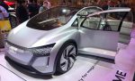
What will the new decade bring us? Will we finally get flying cars? Not likely, but we should see more self-driving cars on the road by the end of the decade. According to CTA, we should also see the beginnings of flying taxis, electric vertical take off and landing (eVTOL) vehicles, which can be summoned for a ride like Uber or Lyft. Bell (top) and Hyundai showed prototypes of these at CES.
Electric cars should become more commonplace in the 2020s. A CES session on electric vehicles predicted electric vehicles (EVs) will have cost parity with traditional cars by 2025. EVs should have average lifetimes of at least 12 years compared to about 8 years for traditional gasoline/diesel cars. Most EVs should have a range of 250 to 300 miles. Growing networks of charging stations will enable recharges in 20 to 60 minutes. Self-driving cars are still in the experimental stage, but by the end of the decade they should be more common on roads. Audi, Hyundai and Toyota were among the companies displaying prototype self-driving vehicles at CES. Toyota display an EV van (e-Palette) which would include robots (Micro Palette) to make the final delivery. Mercedes-Benz displayed its Vision AVTR concept self-driving car. Inspired by the movie Avatar, Mercedes described the vehicle as “holistic, immersive and intuitive”.
CES covers a large range of technology including artificial intelligence (AI), robotics, smart houses, smart cities, digital health, sports technology, travel & tourism, audio/video, virtual reality & gaming, drones, wireless and computing. A large area of CES was devoted to AI and robotics. Numerous robots were on display. Most were limited function robots such as vacuums, window washers, delivery platforms, information kiosks, and toys. There were robot dogs and cats which mimic pets without the feeding, waste disposal and vet bills. We have posted pictures of some of these robots on our website.
Many of the products shown at CES are innovative and potentially useful. Others are questionable as to whether they fill a real need. Some of the more innovative products include a system which uses IR (infrared) signals to power nearby sensors, eliminating the need to charge or replace batteries. An experimental system is aimed at powering remote sensors by harnessing cellular radio signals and other radio waves in the air. A platform for stroke recovery uses a dance type video game. Some of the questionable products include a suitcase which follows you and a diaper with sensors to detect waste (isn’t that what a nose is for?).
We at Semiconductor Intelligence attended the press conferences of Panasonic and Sony and the keynote address by Samsung president and CEO HS Kim.
Panasonic’s press conference promoted the 2020 Olympics in Tokyo where it supplies the displays and other technology at the Olympic Stadium. The conference included an appearance by Olympic swimmer Michael Phelps, who will work with Panasonic along with other athletes. Panasonic supplies the displays used in Disney’s new Star Wars sections of its theme parks in Florida and California. Automotive is a major focus for Panasonic. It is the largest supplier of EV batteries and supplies information and entertainment systems. Panasonic is working with Tropos Motors, which makes EVs including small trucks for deliveries. Panasonic and the state of Utah are developing a transportation data network. Panasonic is the largest supplier of inflight entertainment systems and is developing a system to cancel out airplane engine noise without headphones. The press conference also mentioned Panasonic’s Lumix cameras, professional camcorders, and OLED TVs.
Sony’s press conference pushed its new 8K TVs and 360-degree reality TV. Sony will introduce its latest video game system toward the end of this year. The PlayStation 5 will feature 3D audio, ultra-high speed SSD and ultra HD Blu-ray. In sports, Sony will use 5G to transmit camera images without the need for cabling. The next megatrend, according to Sony, is mobility. They showed a prototype EV car which features Sony CMOS image sensors, a panoramic display, LIDAR, 33 sensors, and software updated wirelessly.
Samsung Consumer Electronics president and CEO Hyun-Suk Kim gave one of the keynote addresses. He emphasized a new “age of experience” where most people will value experiences over products. He demonstrated Ballie, a softball type robot which follows you and can control home functions through voice commands. Samsung showed several health-related products including a Galaxy watch which detects stress and offers stress relief suggestions. An exercise system uses motion capture to evaluate yoga poses and other exercises and suggest improvements. A cardiac rehab system provided home-based guidance using wearables and smartphone. The process is supervised by a remote therapist. Samsung supplies several smart home devices including robotic vacuums and smart refrigerators which can suggest menus and order food. Samsung demonstrated a gait enhancement and motivating system (GEMS) which uses a gadget around a person’s waist and legs along with VR glasses to analyze motion and provide coaching. The GEMS system can also be used in rehab. Samsung is targeting smart cities with energy sensors & controls and 5G telematics for transportation monitoring and control.
The future of consumer electronics is diverse. Vehicle technology and IoT (Internet of Things or Intelligence of Things) will be key drivers. Traditional drivers such as smartphones, televisions, laptop PCs and tablets are reaching saturation. However, smartphones will have a boost in the next couple of years due to 5G and televisions will see growth from 8K displays. Increasing use of AI in electronics should lead to practical self-driving vehicles and more functional robots by the end of this decade. But still no flying cars!


