RVN! 26 Banner revised (800 x 100 px) (600 x 100 px)

FPGAs in the 5G Era!

FPGAs in the 5G Era!
by Daniel Nenni on 01-27-2020 at 6:00 am

New Family of FPGAs Speedster7t

FPGAs, today and throughout the history of semiconductors, play a critical role in design enablement and electronic systems. Which is why we included the history of FPGAs in our book “Fabless: The Transformation of the Semiconductor Industry” and added a new chapter in the 2019 edition on the history of Achronix.

In a recent blog post “FPGAs in the 2020s – The New Old Thing” Achronix reminds us that even though FPGAs are 35 years old the coming age of AI in the cloud represents a new FPGA growth opportunity to which I agree to 100%. In fact, during our first webinar series last year the Achronix ML webinar broke analytic records.

Whether on the edge (eFPGA) or in the cloud (FPGA), programmable technology will play a critical role with the explosive data growth of the 5G era which has just begun.  We started tracking AI on SemiWiki in Q4 of 2015 and have published 182 blogs that have garnered close to one million views which is quite good. We also get to see who reads what, when, and where. Just to net it out, AI is everywhere and companies big and small are consuming AI design enablement information as fast as we can publish it, absolutely.

Back to the Achronix blog post “FPGAs in the 2020s – The New Old Thing”, it is full of interesting data and links that will be of great use if you are investigating FPGA use in the 5G era. I have also spent many hours researching AI and have finished several AI projects in collaboration with some big name companies and SemiWiki partners. Hit me up in the comments section if you want to talk more. AI is coming, there is no stopping it, and it is exciting so let’s talk.

FPGAs in the 2020s – The New Old Thing, January 8, 2020

FPGAs are the new old thing in semiconductors today. Even though FPGAs are 35 years old, the next decade represents a growth opportunity that hasn’t been seen since the early 1990s. Why is this happening now?

There continues to be a data explosion in the world, with IDC predicting over 175 zetabytes of data will be generated annually by 2025. With this much data, there is a tremendous opportunity to analyze it for insights that can change and influence the world. AI will play a huge role in this data mining operation, and companies are growing their workforce with deep skills in machine learning and data analytics to meet the challenges of the future…

And don’t miss the upcoming Achronix webinar:

New Block Floating Point Arithmetic Unit for processing AI/ML Workloads in FPGA

Abstract:
Block Floating Point (BFP) is a hybrid of floating-point and fixed-point arithmetic where a block of data is assigned a common exponent. We describe a new arithmetic unit that natively performs Block Floating Point for common matrix arithmetic operations and creates floating-point results. The BFP arithmetic unit supports several data formats with varying precision and range. BFP offers substantial power and area savings over traditional floating-point arithmetic units by trading off some precision. This new arithmetic unit has been implemented in the new family of 7nm FPGAs from Achronix. We cover the architecture and supported operations of the BFP unit. In this presentation, artificial intelligence and machine learning workloads are benchmarked to demonstrate the performance improvement and power savings of BFP as compared to half-precision (FP16) operations.

About the presenter
Dr. Mike Fitton is senior director, strategy and planning at Achronix. He has 25+ years of experience in the signal processing domain, including system architecture, algorithm development, and semiconductors across wireless operators, network infrastructure and most recently in machine learning.


Tesla is Teaching Us to Move Over

Tesla is Teaching Us to Move Over
by Roger C. Lanctot on 01-26-2020 at 10:00 am

Tesla is Teaching Us to Move Over

Believe it or not, Tesla Motors is teaching us to be better drivers. One of the most remarkable lessons we are learning is that motor vehicles on public roadways ought to stay away from emergency and other service vehicles. In the U.S., we can all expect to hear more about “Move Over” laws – now enacted in all 50 states.

It sometimes seems as if Tesla vehicles have an uncanny ability, while operating in Autopilot mode, to collide with emergency vehicles parked on highways while on official business. The latest incident occurred on December 29th in Cloverdale, Ind., when a Tesla Model 3 collided with a fire truck on Interstate 70. The fire truck reportedly had its lights flashing while parked in the left lane. A passenger in the vehicle was killed. (Coincidentally on the same day in Gardena, Ca., a Tesla Model S also reportedly operating on Autopilot ran a stoplight and crashed into the side of a Honda Civic, killing its two occupants.)

Let’s be clear about one thing. Non-Tesla vehicles get into crashes every day in the U.S. (and around the world) resulting in 100 lives lost daily in the U.S. (3,500 globally). Highway fatalities have become sufficiently routine as to be accepted as the cost of owning and operating our own cars on public rights of way.

Tesla crashes and the associated injuries and fatalities, on the other hand, are news events because the company has introduced computer-based driving into the equation in such a manner as to appear reckless and inspire opposition and outrage. Tesla crashes are also news events because they remain relatively rare.

The unique inclination of Tesla’s operating on Autopilot to collide with emergency vehicles, though, has shown a spotlight on a big problem for which a solution may be in the offing. Last week, U.S. Department of Transportation Secretary Elaine Chao announced the commitment of $38M to equip emergency response vehicles and infrastructure with life-saving V2X technology in the 5.9GHz band. Chao noted that emergency response vehicles are involved in roughly 46,000 crashes, causing 17,000 injuries and 150 fatalities annually.

The First Responder Safety Technology Pilot Program described by Chao will provide funding to equip emergency response vehicles, transit vehicles, and related infrastructure including traffic signals and highway-rail grade crossings with V2X technology. Chao did not specify the nature of the V2X wireless technology but her comments were interpreted to be technology agnostic – though she did note the agency’s preference that 5.9GHz be preserved for transportation applications regardless of the technology.

Chao’s announced plans mirror legislation sponsored by U.S. Senators Dick Durbin (D-IL), and Tammy Duckworth (D-IL) and introduced in 2019 intended to establish a new national safety priority within an existing federal grant program to increase public awareness of “Move Over” laws and encourage implementation of life-saving digital alert technology.

The USDOT’s announcement of these initiatives also follows appropriations language secured by Durbin, establishing a $5M pilot program to test and deploy these digital alert technologies to protect law enforcement, first responders, roadside crews, and others while on the job. (Worth noting a demonstration at CES2020 by Veoneer and Verizon equipping roadside workers with 5G infused safety vests for communication with oncoming vehicles.)

Chicago-based HAAS Alert supports the Senate bill. The company has spent years implementing its vision of a “Safety Cloud” intended to aggregate digital alerts derived from tracking devices mounted on emergency response and service vehicles.

The effort by HAAS Alert to create its safety cloud has taken many forms, but progress has been steady. The goal is to deliver a driver alerting system that might integrate with embedded in-vehicle infotainment systems and or smartphones to warn drivers of emergency vehicles stopped in the road ahead or approaching from behind or even approaching perpendicularly at an upcoming intersection.

On January 6, Haas Alert announced a deal with Oshkosh-Pierce Manufacturing whereby HAAS Alert digital alerting technology will be included as a standard safety feature at no additional cost in Pierce’s custom fire apparatus and as an available aftermarket solution for apparatus currently in service. HAAS Alert struck a similar deal with vehicle maker RevGroup in 2018.

Other HAAS Alert deals and initiatives include:

  • Signed a partnership with Code3, one of the largest emergency vehicle and work truck market light manufacturers
  • Performed a Sprint “5G” test for emergency vehicle to emergency vehicle communication
  • Surpassed 100M driver alerts in September 2019; now in use in more than 90 cities
  • Fire Standards committees: NFPA950/951 added Digital Alerting language into standards. NFPA1901 is in public comment to have a standard for Digital Alerting into the fire space.
  • Integrated head unit digital alerting pilots with multiple automotive OEMs and suppliers
  • First DOT fleets added in 2019 along with utility trucks, a major U.S. Turnpike, DOT snowplows, a large state tollway. All with flashing light vehicles which will send out Digital Alerts to drivers.
  • Awarded Department of Homeland Security contractor for First Responder V2X – already commercialized and deployed
  • NHTSA funded Digital Alerting grant in 2019 for deployment and a study, Michigan’s PlanetM funded deployment of digital alerting
  • Awarded an Air Force SBIR Contract for fleets
  • Co-founder of non-profit (https://www.arrowcoalition.org/ ) to bring awareness of Move Over Laws

HAAS Alert has learned that it isn’t easy to “do the right thing” when it comes to saving lives with driver alerting technology. Secretary Chao’s announcement has created confusion emphasizing, as it does, V2X technology. The HAAS Alert safety cloud is not yet a V2X solution – it is a V-2-cloud-2-V solution today. HAAS Alert has had to create a chipset swappable solution capable of supporting 3G, 4G, LTE, 5G, FirstNet, DSRC, and AT&T and Verizon SIMs. (The HAAS Alert solution does provide for inter-vehicle communications between first responder vehicles.)

To help spread the word on its safety cloud HAAS Alert has published a guide describing both the safety cloud and something the company calls FleetFusion (https://tinyurl.com/tthyd3z). The company also integrates with Geotab and ESRI/ArcGIS platforms: https://www.prnewswire.com/news-releases/haas-alert-launches-on-the-geotab-marketplace-to-offer-enhanced-safety-service-300937015.html

By now it’s clear that first responder fatalities are a problem for all road users, not just drivers of Tesla’s with Autopilot. There were 49 first responders killed in 2019 as a result of 90,000 collisions – the greatest single source of fatalities for this community. Illinois, alone, saw three state troopers die in roadside crashes. The numbers are already on the rise in 2020. Tesla is teaching us to Move Over. HAAS Alert is showing us how… and when.


Woven City: Smashing Toyota’s Looms

Woven City: Smashing Toyota’s Looms
by Roger C. Lanctot on 01-26-2020 at 6:00 am

Woven City Smashing Toyotas Looms

Car companies are interesting creatures in a corporate world increasingly dominated by Internet-centric behemoths from Silicon Valley, Seattle, and China. While the denizens of the Internet have demonstrated their ability to create billions of dollars in shareholder value from the whims and whimsy of browsing consumers, car companies have built their valuations on approximating the desires of their potential customers and selling expensive hardware one unit at a time – usually through networks of dealers.

While Internet-centric companies thrive on instant gratification, building solid foundations of value upon instant consumer feedback, car companies can be seen to be more or less “guessing” what consumers will want or need years in the future – due to the long product development cycle. When car companies get it right they, too, can create massive shareholder value from strong positive responses to their products: the Volkswagen Beetle, the Ford Model T, the Toyota Corolla.

At CES2020, just a few weeks ago, maximum car maker consternation at the future vehicular desires of consumers was on full display with an emphasis on autonomous vehicles and even flying cars. As the maker of the single most popular vehicle of all time, the Toyota Corolla, Toyota was notable for touting its Woven City concept for a living environment enabled by artificial intelligence and ruled by robots and autonomous vehicles.

CES2020 – Toyota presentation of Woven City concept – https://www.youtube.com/watch?v=NME7pGh-7rk

This utopian or dystopian vision, depending on your point of view, reflected Toyota’s  desire to both segregate and weave together different forms of human transportation moving at different speeds: from pedestrians on foot to low-speed micro-mobility systems, to e-Pallette autonomous shuttles. Toyota intends to break ground on this vision at a 175-acre former manufacturing facility in the shadow of Mt. Fuji in 2021.

In a press event at CES2020 Toyota’s CEO, Akio Toyoda, described the Toyota Woven City vision as a testing facility populated with as many as 2,000 citizens and accessible to scientists from Toyota as well as third parties to test new urban dwelling and transportation concepts. An appreciative audience warmly greeted Toyoda’s conceptual vision, but perhaps they were simply being polite. The implications of Toyota’s Woven City are both troubling and promising and CES2020 attendees can be forgiven for recognizing innovation.

Toyota is to be applauded for affirmatively proposing a solution to the challenges of supporting human life with all of the economic, energy, and ecological concerns currently confronting policy makers and governments. It is no surprise that Toyota emphasizes hydrogen fuel cells at the heart of its vision along with e-Palette autonomous shuttles.

Toyota was kind enough to create a CGI-type rendering of life in the Woven City showing a complete absence of individually owned and operated vehicles – which have been replaced by e-Pallette shuttles. E-Pallette shuttles are also used as delivery vehicles and mobile retail and service delivery platforms in this city of the future.

Perhaps the strangest aspect of the Woven City video is that the kind of walkable urban space that is imagined looks almost identical to the existing walkable spaces created in the typical Tokyo landscape of today. Tokyo itself is a highly walkable city, with wider pedestrian areas – above and below ground – created for shopping, dining or nightlife. It is almost as if Toyota is trying to compete with and/or replace a cityscape that is already functioning effectively.

We can forgive Toyota for focusing so narrowly on the promotion of its e-Pallette concept in addition to hydrogen propulsion. There are many experts and analysts forecasting a future dominated by autonomous shuttles – but few such visions have suggested the complete exclusion of individually owned vehicles.

More remarkable, from the video shared at CES2020, was the division of transportation below and above ground. In the Woven City vision, utilities and product deliveries are managed below ground, while all people moving appears to take place above ground. In fact, the video shows very little people moving taking place.

It is hard to accept this Toyota vision of the future from a nation where the subway system in the nation’s capital, Tokyo, moves more than eight million riders daily. The Woven City has no such subway system in addition to having no cars.

But let’s assume, for a moment, that e-Pallette’s will take on the role of people moving. This raises the question of what the future of Toyota’s vehicle marketing will become. Does the Woven City suggest a future of Toyota selling commercial vehicles in the form of autonomous e-Pallette’s to developers and cities?

It is worth bearing in mind that Toyota has a majority owned subsidiary – Toyota Housing Corporation – that is in the business of building detached houses and housing products for Japanese consumers. It’s not clear whether the Woven City vision represents an extension of this corporate vision, but it is worth noting – especially given the fact that Toyota Home stores can be found in most Japanese cities.

The only criticism of the Woven City expressed in press reports came in reference to potential privacy violations or to the process of selecting the up-to-2,000 residents of the city. All in all, the entire venture appears far too artificial to address relevant challenges facing urban leaders around the world today.

Transportation is at the core of many of the woes facing cities today. Many of the largest urban centers on the planet have maxed out their ability to accommodate individually owned and operated motor vehicles and are putting policies in place to pry people out of their cars.

The latest initiatives include selling transportation as a subscription or service packaged in segments of hours or days or weeks and aggregated across multiple means of transportation – with an emphasis on public/shared resources. Some cities in the U.S., Europe, and elsewhere have gone further by making public transportation of one kind or another – buses in particular – entirely free.

These strategies, intended to leverage existing infrastructure at minimal cost and maximum impact, are beginning to alter consumer behavior – de-emphasizing the automotive default. Toyota’s Woven City, like its hydrogen propulsion obsession, appears completely detached from current realities with no evolutionary path to adoption. And the exclusion of existing mass people movement solutions is particularly glaring coming from a country that is arguably a leader in the massive and high speed movement of people.

Near the end of his presentation, CEO Toyoda notes Toyota’s legacy as a manufacturer of looms, a heritage shared by many other large Japanese electronics companies some of which, like Nakajima and Brother, first made sewing machines. Sad for me to say, the Woven City looms as a detached dystopian vision of future living that must be reconsidered in the context of current mass public transportation needs.

More compelling, though arguably more complex, is the almost simultaneous announcement from Toyota of the launch of its Kinto car subscription and mobility portfolio in Europe. This multifaceted approach to expanding transportation options offers the prospect of having an immediate impact on the ownership and usage of existing vehicles. This is probably worth a closer look and more attention than the Woven City. More details can be found here: https://newsroom.toyota.eu/toyota-launches-kinto-a-single-brand-for-mobility-services-in-europe/


ASML “A Swing to Memory Looms” Nice performance while awaiting Memory bounce

ASML “A Swing to Memory Looms” Nice performance while awaiting Memory bounce
by Robert Maire on 01-24-2020 at 6:00 am

ASML 2020 Logic Memory
  • Good Q4 & 2019 despite weak memory
  • 2020 will be up year but memory an unknown
  • EUV ramp is on track – no China or memory impact
ASML reports an “in line” Q4 despite industry weak 2019

ASML reported sales of 4B Euros and a nice gross margin of 48% resulting in 2.70 Euros per share in earnings.  Orders came in at 2.4B Euros with roughly 80% coming from logic. Despite 2019 being a down year for semiconductor equipment as a whole, ASML managed to have 8% growth during 2019 as spending in the industry shifted back towards lithography purchases,  We expect this trend of enhanced litho spending to hold true in 2020 as the industry continues its EUV adoption.

Logic (TSMC) remains the biggest driver at roughly 80%
It is interesting to note that ASML was able to keep up its growth despite the fact that memory spend went from the majority of sales in 2019 down to roughly 20% of sales at the close of the year. Despite this huge shift in end market demand the company has maintained good growth.

It obviously helps a lot to have strong backlog and a strong order book to be able to more efficiently manage the ebbs and flows of customer mix as 2019 was not an ebb and flow but more of a stampede away from memory to logic/foundry. It also helps that EUV is obviously focused on foundry/logic so the stampede was to ASML’s benefit as well.

“Focus” changes from making EUV work to making more EUV…..
It is also very clear that now that we are well over the acceptance and HVM hurdle of EUV, attention is now turning to turning out more systems faster. Getting down cycle times and getting the supply chain cranked up while still hard is not as hard as working out the kinks has been over the last few years.

2020 looks to be about 35 EUV tools with an eye towards 50 in 2021.  These seem like reasonable, “doable” targets.  We don’t think we need a full blown memory recovery to get to this years goal of 35 and memory will likely recover soon enough to support a 2021 goal of 50.

There is still a lot of work to be done on high NA but less critical than the original work as high NA is an improvement rather than wholesale change.

Multibeam delay helps KLA
One of the few negative points raised, although minor, was the delay of multibeam.  While not totally unexpected given the complexity, it does give KLA a bit of time to work on their products and counter measures.

In our view now that the war has been won on EUV, ASML can and should shift some more focus and spend to metrology & yield related issues and tools and products as it will also support the infrastructure for EUV going forward.

Memory still an unknown
It was clear from the call and clear in our view that the recovery of the memory industry is very much unclear. While NAND will no doubt recover first and DRAM some time later, the company gave no indication other than “just hoping” that memory recovers.  There was no evidence given nor implied of improved order activity or any other indication of memory spend coming back any time soon.

Like the rest of the industry, the key to a strong up cycle is memory along with foundry/logic both working at the same time….we remain with foundry/logic at roughly 80% of business with memory barely plodding along. This is obviously more of a negative for players like Lam who are much more memory centric.  Even though business at Lam and Applied has picked up of late, its not like the rip roaring memory love fest.

China is a non-issue
There remains a lot of discussion in the press about poor ASML being the ping pong ball in a game between China and the US.  So far we see zero impact from any sales restriction to China.  We expect no near term ill effects on ASML and the real issues and impact are more political than financial.  Though ASML may not be happy to be a pawn it hasn’t impacted their profitability or overall sales. We think there is a higher level of risk of the embargo spreading to US equipment companies that would see more financial impact.

The stocks
Given that the quarter was just in line with no surprises, we expect little movement in an already fully priced stock. There was also nothing surprising nor significantly impactful on other stocks that would drive the group one way or another.  The lack of any sign of memory recovery is a little bit disappointing for the group that has seen its shares on a tear despite the weakness.

All in all no impact and we are not motivated to run out and chase stocks that have already run up nor are we tempted to short stocks that have such unusual support.


US China Trade Deal – Will it Work?

US China Trade Deal – Will it Work?
by Gordon Orr on 01-23-2020 at 6:00 am

China US Trade deal Will it Work

A signed trade deal between the US and China has finally been signed. How much does this settle down the relationship and what will continue to cause problems? Given that in the same week as the deal was signed, the US government confirmed their new tough restrictions on allowing Chinese investment at any level into technology and many other sectors deemed sensitive in the US, clearly not all is well.

For companies manufacturing in China, we have the benefit of certainty of what tariff levels we need to deal with.  If exports are in the 7.5% tariff category that’s low enough that we might just keep manufacturing in China. For multinationals with sophisticated supply chains and factories all around the world, their executives simply put the tariff costs into their models and determine whether Mexico, Turkey, Vietnam or China is now the best place to produce products for China. The losers in all this are smaller companies that perhaps only had 1 factory in China and who sold most of their output in the US. Shifting production is enormously disruptive and they may not even have the skills to do so. With clarity on tariffs, expect an uptick in investment in factories in China as companies move ahead with investments that had been on hold.

China has agreed to purchase US$200bn over a 2017 base line from the US. How hard will that be and who wins and loses?

·        Manufactured goods: Provided Boeing is able to get the 737Max recertified in China sometime in the next 2 years, simply clearing the backlog on these planes ordered by China will generate many billions of incremental sales. Certainly, China will be willing to buy more technology products such as semiconductors from the US – but there may be friction on this if the US restricts the ability of Chinese companies to buy these products. China can buy more oil from the US, if the US actually has the capacity in its ports to enable this. China has a surplus of refining capacity and could import US oil to fill these refineries who will simply turnaround their output and export it. Winners – Chinese refineries, losers – refineries elsewhere in Asia. Automotive exports from the US to China are modest and not likely to grow much. Chinese consumers aren’t very interested in US style pick-up trucks. GM makes China specific cars in China; Tesla manufactures in China. The largest exporter of auto from the US to China is probably Mercedes.

·        Agricultural products. Probably the most important category for the Trump administration to see progress on in 2020. Soya beans and other cereals, beef and pork, premium fruit and vegetables. Winners US agricultural producers, losers South American producers and possibly Chinese consumers who may end up paying higher prices if US goods are not cost competitive in global markets.

·        Services. Again, there could be much friction here. China could say: “We are encouraging more Chinese tourists to visit the US and students to study in the US, but you, the US, won’t give them visas”. Chinese companies will be very willing to license US technologies, brands and other IP, but will CFIUS allow them to do so?

So yes, there is a path to achieving the $200B – but it requires constructive engagement from the US, as much as from China.

China also agreed to accelerate opening up financial services and other sectors to US companies, with faster issuance of licenses to operate. China made clear today that this opening is to companies of any nationality, not just American. Many of the announced moves on IP protection and technology transfer were contained in the new Foreign Investment Law which went into effect a few weeks ago.

The trade deal does nothing to address the growing separation in many areas that both governments seem to be pushing for. In brief, restrictions on Chinese investments in US technology startups, in financial services, in any business that capture personally identifiable information will all be harder. Exports of technology products and IP from the US to China will be harder and China will continue to seek to become more self-sufficient. Market access in the US for Chinese technology companies will diminish further. China’s “secure and control” policy domestically will likewise reserve more of its technology market for Chinese companies. Chinese researchers will find it harder to obtain and retain positions at US universities or even in leading US tech companies. Chinese and US versions of product standards will emerge. The Chinese and US internets will continue to diverge and may eventually even lose interconnectivity. The threat to delist Chinese businesses currently trading on US stock exchanges remains real.

The trade deal does remove some uncertainties, allowing companies to move forward with their investment plans for manufacturing. It will lead to greater purchases by China from the US, but not without creating significant frictions. And it does nothing to shift the direction of travel towards separation on flows of capital, of talent, of IP and of technology based goods


Using IMUS and SENSOR FUSION to Effectively Navigate Consumer Robotics

Using IMUS and SENSOR FUSION to Effectively Navigate Consumer Robotics
by Daniel Nenni on 01-22-2020 at 10:00 am

Ceva Webinar iRobot SemiWiki

There is a live CEVA webinar coming up that you will NOT want to miss. We have been working with CEVA since 2012 and have posted 130 collaborative blogs. Those blogs have earned 927,901 views thus far and counting. The average blog on SemiWiki.com gets 5,885 views so they are ahead of the game.

One of the reasons CEVA is so popular on SemiWiki is due to the rising interest in commercial semiconductor IP from the electronics systems companies who are now doing their own chips.  Another reason is that CEVA provides some of the best background materials we get on SemiWiki.

Additionally, CEVA is staffed by some of the smartest and most humble semiconductor professionals that we have the fortune to work with. A very good combination for a media portal partner, absolutely.

REGSTRATION

Abstract

Robotics is a field that is growing rapidly. In particular, consumer ground-roving robots are becoming mainstream now that they commonly incorporate more intelligent navigation to operate more autonomously. Inertial measurement units (IMUs) are sensors that are essential for achieving precise navigation. IMUs can be used as a primary sensor for navigation or as a complementary sensor that helps VSLAM systems achieve robust performance. But making use of IMUs requires deep understanding of their idiosyncrasies and modeling to assess their impact. In this webinar, engineers will learn about the challenges when working with IMUs, how IMUs are applied in different robotics applications, and what is necessary to test IMU-based robots to achieve great performance.

Join CEVA’s experts to learn about:

  • Consumer Robot Vacuum Industry Overview
  • Common home robot navigation paradigms
  • Sensor idiosyncrasies and the importance of qualifying sensors
  • How to maintain accuracy over time, temperature, and environment
  • How to create robust algorithms and verify performance
Target Audience

Design, system, and product engineers looking to enhance their understanding of IMUs, sensor fusion, and how they relate to SLAM. Robot OEMs interested in navigation for their ground-roving robots.

Speakers
Charles Pao
Sr. Marketing Specialist, Sensor fusion BU, CEVA

Steve Scheirey
Sr. Director, Software, Sensor fusion BU, CEVA

About CEVA, Inc.
CEVA is the leading licensor of wireless connectivity and smart sensing technologies. We offer Digital Signal Processors, AI processors, wireless platforms and complementary software for sensor fusion, image enhancement, computer vision, voice input and artificial intelligence, all of which are key enabling technologies for a smarter, connected world. We partner with semiconductor companies and OEMs worldwide to create power-efficient, intelligent and connected devices for a range of end markets, including mobile, consumer, automotive, robotics, industrial and IoT. Our ultra-low-power IPs include comprehensive DSP-based platforms for 5G baseband processing in mobile and infrastructure, advanced imaging and computer vision for any camera-enabled device and audio/voice/speech and ultra-low power always-on/sensing applications for multiple IoT markets. For sensor fusion, our Hillcrest Labs sensor processing technologies provide a broad range of sensor fusion software and IMU solutions for AR/VR, robotics, remote controls, and IoT. For artificial intelligence, we offer a family of AI processors capable of handling the complete gamut of neural network workloads, on-device. For wireless IoT, we offer the industry’s most widely adopted IPs for Bluetooth (low energy and dual mode), Wi-Fi 4/5/6 (802.11n/ac/ax) and NB-IoT. Visit us at www.ceva-dsp.com and follow us on TwitterYouTube, FacebookLinkedIn and Instagram.

Also Read:

A Bundle of Goodies in Bluetooth 5.2, LE Audio

Glasses and Open Architecture for Computer Vision

Location Indoors: Bluetooth 5.1 Advances Accuracy


Formal and High-Level Synthesis

Formal and High-Level Synthesis
by Bernard Murphy on 01-22-2020 at 6:00 am

SLEC verification

Formal verification has made significant inroads in RTL and gate-level verification because it provides complementary strengths to conventional dynamic verification methods; using both provides higher levels of coverage and confidence in the correctness of an implementation. I haven’t heard as much about formal use in high-level synthesis (HLS) flows so was interested to see a white paper from Renesas on how they use Catapult formal tools in this context.

First, why even use formal in such a flow? One reason is obvious. When you synthesize from one format to another, from C++ to RTL or from RTL to gates, no amount of simulation is going to prove conclusively that synthesis didn’t introduce some subtle error along the way. That’s why equivalence checking was invented, to prove that at minimum the input and output implementations are functionally equivalent at a cycle-level.

Another reason is to do some level of formal checking on the C++ itself. A couple of examples are out-of-range-accesses on arrays and uninitialized memory reads. You might catch these in C++ simulation, but you might not. Experienced programmers know that behind rarely taken branches can lurk dragons; formal is a good way to expose such problems. And the beauty of these methods is that they not only discover that a problem is possible, but they also show you how to create that problem, which should make it easier to figure out a fix.

Still, the bulk of Renesas’ usage is in equivalence checking and this starts with C++ to C++ checks. Renesas talks about image processing IP and communication IP, both natural applications for HLS. Both types of design are intrinsically complex and will evolve through multiple iterations. Equivalence checking between C++ revs can assure as completely as possible that unintended functional changes are not introduced.

This is sequential equivalence checking and will not always get to a proof of equivalence (or no-equivalence) without a little assistance. What will push a proof towards convergence in these cases is more hints (constraints) on behavior, such as bounding the range of an apparently unbound array index.

The best-known application of equivalence checking in HLS flows is in comparing the source C++ with the synthesized RTL. There’s an advantage here (I’m guessing) in having the HLS synthesizer and the SLEC equivalence checker come from the same product group. The checker knows what kinds of transformations the synthesizer can make, such as how it inserts pipeline stages, and can factor these in when looking for a complete proof.

I believe based on my reading of the Renesas white paper that they only edit the source C++, so all RTL changes are based on re-synthesis from source updates. They run equivalence checking on each RTL drop to establish either that they can get to a full proof or to find any bottlenecks to getting to proofs. This is with the goal of ensuring a full proof by the time they get to the final RTL drop.

Methods to help along full-proofs at this level are pretty familiar – help in identifying equivalence points between the two designs, along with some level of abstraction and hierarchical proving.

Renesas results are impressive in comparison with verification through extensive simulation. They show one example, for an image processor IP, in which they were able to reduce turnaround time from 260 days (simulation-based) to 4 days using equivalence checking. Of course you still want to do lots and lots of simulation (in C+) to prove functionality and performance. Catapult SLEC removes the need to worry about implementation bugs being introduced in mapping from C++ to RTL.

You can read the Renesas white paper HERE.


Qualcomm introduces Snapdragon 720G, 662 and 460 SoCs with Wi-Fi 6, NavIC Support

Qualcomm introduces Snapdragon 720G, 662 and 460 SoCs with Wi-Fi 6, NavIC Support
by Raju Prasad on 01-21-2020 at 10:00 am

Snapdragon NavIC SoC 768x519

Qualcomm today announced three new chipsets for entry level and mid-range smartphones – Snapdragon 720G, Snapdragon 662, and Snapdragon 460. The first one promises to bring many of the Elite Gaming features of the 765G with support for HDR, dynamic color range and high-quality synchronized sound with Qualcomm aptX Adaptive.

The SD662 will bring triple-camera support, which is a first for a Qualcomm 6-series chipset. Snapdragon 460 might be most affordable of all three, but still will be able to provide an increase in CPU and GPU performance over other 4-series chipsets.

According to Rajen Vagadia, president of Qualcomm India, the chip maker is introducing these three platforms for 4G markets where seamless connectivity access is still unraveling. Kedar Kondap from the product management team of the San Diego company confirmed the 720G, 662, and 460 will be able to provide gaming experience at a more affordable price.

Senior executives of smartphone companies such as Manu Kumar Jain at Xiaomi and Madhav Sheth at Realme confirmed they will “work closely” with Qualcomm to introduce phones with the new chips, including the most interesting of all three – Snapdragon 720G.

                      Snapdragon 460 (11nm)

Key features:

  • CPU – 8x Kryo 240 cores up to 2.3GHz
  • GPU – Adreno 610 GPU
  • DSP – Hexagon 683 with vector extensions, hardware-accelerated TensorFlow Lite
  • ISP – Spectra 340 ISP supporting 25MP camera, or dual 16MP camera
  • Connectivity
  • Cellular – Snapdragon X11 LTE modem
  • WiFi 6 ready
  • Bluetooth 5.1 with advanced audio via the Qualcomm FastConnect 6100 platform
  • GNSS – Dual-Frequency (L1 and L5) GNSS for GPS, Galileo, GLONASS, Beidou, NavIC
  • Quick Charge 3.0 – 0 to 50% in 20 minutes
  • Process – 11nm

Snapdragon 460 is an update to the Arm Cortex-A53 based Snapdragon 450 processor with the custom Kryo 240 processor delivering up to 60% extra performance, while Adreno 610 GPU delivers up to 70% performance increase over Adreno 506.

                      Snapdragon 662 (11nm)

Highlights:

  • CPU – Octa-core “Kryo 260” processor with four Cortex-A73 cores @ up to 2.0 GHz, and four Cortex-A53 cores @ up to 1.8 GHz
  • GPU – Adreno 610 GPU
  • DSP – Hexagon 683 with vector extensions, hardware-accelerated TensorFlow Lite
  • ISP – Spectra 340T ISP supporting 48MP cameras, HEIF capture, and triple cameras
  • Connectivity
  • Cellular – Snapdragon X11 LTE modem
  • WiFi 6 ready
  • Bluetooth 5.1 with advanced audio via the Qualcomm FastConnect 6100 platform
  • GNSS – Dual-Frequency (L1 and L5) GNSS for GPS, Galileo, GLONASS, Beidou, NavIC
  • Quick Charge 3.0 – 0 to 50% in 20 minutes
  • Process – 11nm

Snapdragon 662 looks very similar to Snapdragon 665, but with a slower modem, and better ISP. It also shares many features of Snapdragon 460, but with more powerful Cortex-A73 CPU cores, and better camera support.

                     Snapdragon 720G (8nm)

Key features and specifications:

  • CPU – Octa-core “Kryo 465” processor with 2x Cortex-A76 cores @ up to 2.3 GHz, and 6x Cortex-A55 cores @ up to 1.8 GHz
  • GPU – Adreno 618 GPU
  • DSP – Hexagon 692 Hexagon Tensor Accelerator
  • ISP – Spectra 350L ISP supporting 192MP cameras, HEIF capture, and 4K video capture
  • Connectivity
  • Cellular – Snapdragon X15 LTE modem
  • WiFi 6 ready
  • Bluetooth 5.1 with advanced audio via the Qualcomm FastConnect 6200 platform
  • GNSS – Dual-Frequency (L1 and L5) GNSS for GPS, Galileo, GLONASS, Beidou, NavIC
  • Fast Charging – Quick Charge 4+ allowing 0 to 50% charge in less than 15 minutes; USB PD support
  • Process – 8nm

Snapdragon 720G looks to be an upgrade to Snapdragon 712  with the processor delivering a 60% performance increase, and the GPU providing 75% better improve and support for HDR video playback.

Availability

Snapdragon 720G based phones will come to market soon as the first devices are slated for Q1 2020, but we’ll need to wait a little longer for Snapdragon 662 and Snapdragon 460 based smartphones which are scheduled for the end of 2020

Via Press Release

Raju Prasad


IEDM 2019 – Imec Interviews

IEDM 2019 – Imec Interviews
by Scotten Jones on 01-21-2020 at 6:00 am

Slide4

Imec is one of the premier semiconductor research organizations and at IEDM they presented dozens of papers. I had the opportunity to see several of the papers presented and interview 3 of Imec’s researchers.

Jan Van Houdt, DMTS ferroelectric and exploratory memory

I have had very interesting discussions with Imec researchers about memory trends in the past and I asked to interview an Imec memory expert at IEDM this year. Jan Van Houdt has been Imec’s chief scientist and is now DMTS ferroelectric and exploratory memory. My interview with him wasn’t so much tied to specific Imec papers but rather a general discussion of the state of memory.

DRAM scaling has slowed and is facing very difficult issues. Last year at IEDM Imec presented work on Strontium Titanite (STO) dielectric for DRAM with higher K values that could potentially enable capacitor shrinks. He said they still hadn’t met all the specifications for k value, thickness and leakage and they are still trying to add elements to the films to address this. I asked him what he thought would be the long-term replacement for DRAM and he said they thought they could get Ferroelectric based memories to cost and density parity with DRAM but endurance is the key limiter. I was surprised by this, I thought Ferroelectric based memories were really just a niche memory but he was very optimistic about the future of Ferroelectric memories and that is why he has made it his focus. The current Ferroelectric material of choice is HfZrO4 with an endurance of 1E11 cycles.

Authors notes, DRAM replacement endurance needs to be >1E15 cycles. Of the current emerging memory types only MRAM and Ferroelectric have good endurance, PCRAM and RRAM are <1E8 cycles. MRAM can potentially have very good endurance but the high switching current requires large selector transistors limiting scaling.

If Ferroelectric can’t replace DRAM as main memory it could be a storage class memory option. He noted that 3D XPoint, a current storage class memory option is too expensive for the performance it offers.

With respect to 3D NAND scaling he mentioned that as the number of layers increases in 3D NAND memory, that the channel resistance becomes an issue. Imec has previously presented work on InGaAs as an alternative to the current polysilicon channels to provide lower resistance. In the original work the InGaAs was in direct contact with the ONO (Oxide-Nitride-Oxide) layer and had a bad interface. They are trying high pressure anneals and looking at ALD deposition. Ideally, they want to use ALD to deposit a crystalline channel. There is currently work being done in the industry to provide a crystalline silicon channel in place of the polycrystalline channel, with epitaxial growth or recrystallization being investigated. To-date epitaxial growth is too slow and expensive and NiSi recrystallization is slow and the Ni stays in the wafer.

There is also a lot of work being done to replace the W word line material in 3D NAND with a lower resistance alternative. They are looking at TiN to fix the channel work function and then Ru fill or Ru without TiN, Mo is also on the list. The switch to an alternate material will be driven by the need to reduce the layer thickness.

Authors note, as an expert in fabrication costs I think Ru will be much too expensive to implement in 3D NAND especially since the deposition is surface area driven and the surface area with a hundred or more word line slots to fill is very high and drives a lot of precursor consumption.

Imec has completed their work on STT MRAM and they are now focused on SOT MRAM using VCMA – Voltage Controlled Magnetic Anisotropy to switch without current. STT must run current through the Magnetic Tunnel Junction (MTJ) for reading and writing. SOT has no current through MTJ, you run the current near it to write but still need to run current through the MTJ to read it. SOT is a three terminal device, so bigger but can switch in 300 picosecond giving SRAM speed. They don’t have the endurance yet; it is early to talk reliability. In theory should be better than STT, STT is 1E10 to 1E12 but some bits fail earlier.

In Ferroelectrics they can do a FET that is a NAND cell and can provide thinner layers for 3D NAND. With InGaXOx they can do a 2T1C (2 transistor – 1 capacitor) memory cell for DRAM like memory, it has a very small capacitor because it is amplified can be in the Back End Of Line (BEOL). They can also try 1T1C (current DRAM standard) or 2T0C and use a parasitic capacitance. He thinks 2T1C is the most interesting.

Christopher Wilson, manager, nano interconnect program and BEOL integration

In this interview we discussed the paper: “Three-Layer BEOL Process Integration with Supervia and Self-Aligned-Block Options for the 3 nm Node”

This paper is an extension of work presented at the IITC conference where they showed 2-layer Ru with metal 2 at a 21nm pitch, the new work adds a 3rd metal layer. In order to achieve a 21nm pitch you need 2 block masks and they used self-aligned block. This work was done on a SRAM so it has a regular layout. The addition of metal 3 allows them to look at stacked vias. Landing via 2 on metal 2 is normally a critical design rule for Cu, the yield didn’t change much with island size. With 3 layers they can also look at super vias with a via from M3 to M1. Authors note super vias are when vias skip metal layers so instead of connecting metal n to metal n-1 you can connect to n-2, n-3 or more.

This paper was all based on ALD deposition of Ru, Co CVD deposition showed gaps. They have newer data on CVD of Ru but this is all ALD based. The ALD Ru deps were 3 hours per wafers and topped with PVD so a CVD or faster ALD deposition will be needed for production.

One important layout dimension in routing is the metal line tip to tip dimension that you want as small as possible. For Cu typically tip to tip is the same as the pitch so for a 21nm pitch, the tip to tip would be 21nm. In the paper they show no change in yield for a tip to tip of 18nm versus a tip to tip of 9nm and the 9nm is actually around 5nm. Ru has 30% better RC (Resistance-Capacitance) than Cu at these pitches.

For M3 the pitch is 36nm and that shows a 10x RC improvment versus M2 at 21nm.

Naoto Horiguchi, Director of CMOS device technology

In this interview we discussed four Imec papers.

First up was “Novel forksheet device architecture as ultimate logic scaling device towards 2nm”

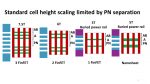
The forksheet is a advanced version of a horizontal nanosheet (HNS) where a dielectric sheet is placed between the nFET and pFET.  Because of how HNS are fabricated they can end up with a larger n to p spacing than a FinFET. The additional of the dielectric wall acts as an etch stop layer. Figure 1 illustrates the effect of n to p spacing on standard cell size.

Figure 1. N to P spacing effect on standard cell size.

Figure 2 illustrates how a dielectric wall in a forksheet mitigates the n to p spacing.

Figure 2. Forksheet dielectric wall mitigates n to p spacing issues.

A forksheet is essentially a FinFET rotated 90 degrees so the electrostatic are not as good as a standard HNS. Recessing the channel during dielectric wall formation can help recover some electrostatic performance. The dielectric wall reduces miller capacitance and can yield 10% higher speed or 24% lower power.

N to p boundary is typically 2x the Fin pitch, the dielectric wall reduces this. For example a 5 track height cell can be reduced to a 4.3 track height cell with the dielectric wall, see figure 3.

Figure 3. Cell scaling advantage for forksheet with dielectric wall.

He believes that the forksheet provides a minimum 20% area improvement.

The second paper we discussed was: “Variability sources in nanoscale bulk FinFETs and TiTaN- a

promising low variability WFM for 7/5nm CMOS nodes”

TiTaN si a potential work function material for controlling threshold voltages (Vt). They deposited it on a high-k dielectric and compared it to TiN and TiN with a SiH4 soak. The SiH4 soak of TiN kind of dopes some silicon atoms on the surface and reduces crystallization improving variability and Vt shift. TiTaN showed a significant further reduction in variability, it is a more amorphous material. TiTaN can be deposited by ALD and can be used on n or p although on p a TaN barrier is needed to block from TiAl.

The third paper we discussed was: “3D-carrier Profiling and Parasitic Resistance Analysis in NW h-GAA CMOS Transistors”

In this work a diamond tipped atomic force microscope is as a scalpel to remove material while also running a spreading resistance probe and create a 3D map of conductivity.

What was found is that dopant diffusion is slow in HNS at the S-SiGe interface.

Authors note, HNS are fabricated as alternating layers of Si and SiGe where the SiGe is a sacrificial layer that gets removed later.

This reduced diffusivity effect will become more important as devices scale and it can impact interface resistance. The ability to measure conductivity at a nanoscale enable better modeling and fundamental understand for future device development.

The final paper we discussed was: “Vertical Nanowire and Nanosheet FETs: Device Features, Novel Schemes for Improved Process Control and Enhanced Mobility, Potential for Faster & More Energy Efficient Circuits”

Vertical nanowires (VFET) are very good for regular layouts such as SRAM or MRAM selectors but not as good as HNS for random logic. This work continues previous Imec work on these devices to further refine the fabrication and performance.

In this work a sacrificial SiGe sleeve is used to introduce stress, the sleeve is fabricated introducing stress and then later removed. This work also showed improved alignment control with a partially self-aligned technique using spacers.

This work could be very interesting for fabrication of highly optimized SRAM chiplets to integrate with logic using 3D packaging techniques. I also found the MRAM selector option very interesting. As I mentioned earlier in this article MRAM selector size is relatively large and limits MRAM scaling. Figure 4 illustrates density improvements by using VFET versus a FinFET.

Figure 4. VFET MRAM selector area advantage versus FinFET.

Conclusion

Imec continues to be a premier research organization in Semiconductor devices and process technology. Innovations such as VFET and Forksheet HNS provide promising options for future scaling. More fundamental work such as understanding carrier profiles in 3D and new work function materials are also key enablers.


TSMC Q4 2019 “2020 Bellwether” Conference Call Summary

TSMC Q4 2019 “2020 Bellwether” Conference Call Summary
by Daniel Nenni on 01-20-2020 at 6:00 am

TSMC Manufacturing Excellence

After returning from a week in Southern China I found the TSMC Q4 2019 conference call even more interesting. In China they are preparing for the New Year’s Celebration so everything is very festive but what struck me hardest was the massive investment in infrastructure and security. Semiconductors are of course a big part of that thus the urgent need for China to be semiconductor-self-sufficient, absolutely.

TSMC of course is a valued partner of China and will benefit the most from China’s continued semiconductor boom. If you read between the lines of the TSMC Q4 conference call you will see it more clearly. First let’s look at the technology parts of the prepared statement:

16-nanometer and below, accounted for 56% of wafer revenue, up from 51% in the third quarter. On a full year basis, 7-nanometer contribution increased from 9% in 2018 to 27% of wafer revenue in 2019. 10-nanometer was 3% and 16-nanometer was 20%. Advanced technologies accounted for 50% of total wafer revenue, up from 41% in 2018.

It is interesting to note that TSMC 20nm and 16nm shared fabs where 20nm was the sacrificial lamb and 16nm is the cash cow. It was the same with 10nm and 7nm (cash cow). So, what is going to happen now that TSMC is moving 7nm customers to 6nm and 5nm is ramping up this year? Will TSMC break the cycle and have two cash cows in a row? From what I have been told 6nm is an EXCELLENT process and will be VERY competitive on price / performance with both TSMC and Samsung 5nm. In fact, my guess is that TSMC 6nm will even outperform Intel 10nm on density, yield, and most certainly cost.

Now let’s take a look at revenue contribution by platform…. On a full year basis, smartphone and IoT led the growth with 12% and 33%, respectively, while HPC, automotive and DCE decreased 8%, 7% and 8%, respectively… Overall, smartphone accounted for 49% of our 2019 revenue; HPC, 30%; and IoT, 8%.

Remember, in 2019 China is second in TSMC revenue (20%) behind the US (60%) but well in front of the other parts of the world and China revenue is on the rise. My guess is that China will be 25% of TSMC’s revenue in 2020 further out pacing Japan, Korea, Taiwan, and the EU, who are all in single digits.

The TSMC smartphone and IoT surge are a very good reflection of the China market.

Samsung is being pushed out of china leaving Apple as the only foreign smartphone supplier in the top 5. Huawei is dominating and Huawei and TSMC go together like peanut butter and jelly. In order to compete the other China smartphone suppliers are forced to follow Huawei into the TSMC ecosystem so it is all about TSMC.

IoT is the interesting one. The number one IoT driver in China is security (cameras) which are EVERYWHERE and backed by AI. 5G is a national priority in China and will increase the abilities of AI on the edge.

For example, in the US we have license plate readers so our local police can identify and recover stolen cars and the criminals that are driving them. The next level is facial recognition where law enforcement can identify known criminals and recover them. China is already at that next level, semiconductors and AI are everywhere and there is no stopping it no matter how you feel about privacy.

We raised our 2019 CapEx guidance by $4 billion to $14 billion to $15 billion, and we ended up spending $14.9 billion. Our 2020 capital budget is expected to be between $15 billion and $16 billion. Out of the $15 billion to $16 billion CapEx for 2020, about 80% of the capital budget will be allocated for advanced process technologies including 3, 5 and 7-nanometers, about 10% will be spent for advanced packaging and mask-making and about 10% for specialty technologies.

As I mentioned before, TSMC won the 7nm, 6nm, and 5nm popular vote so do not be surprised if CapEx is again raised and we have another hockey stick of growth in Q4.

For the full year of 2020, we forecast the overall semiconductor market growth excluding memory to be 8%, while foundry industry growth is forecast to be about 17%. For TSMC, we are confident we can outperform the foundry revenue growth by several percentage points in U.S. dollar term.

Now that ‘s what I’m talking about… 20% growth. It really is satisfying when hard work pays off.

Now allow me to talk about our N5 volume production. Our N5 technology is a full node stride from our N7, with 80% logic density gain and about a 20% speed gain compared with 7-nanometer. N5 will adopt EUV extensively and is well on track for volume production in first half this year and with good yield.

Finally, I’ll talk about our N3 status. We are working with customers on N3’s design, and the technology development progress is going well. We have many technology options in development and we carefully evaluate all the different approaches. Our decision is based on technology, maturity, performance and cost… We will announce more details about our N3 technology at our TSMC North America Technology Symposium on April 29.

TSMC N3 will again be FinFET based. We can talk more about this after the Symposium. The Q&A was pretty lame this time but here is the best answer:

But I can just tell you that whatever you read on the newspaper is not true…