webinar banner2025 (1)

Cadence Dives Deeper at Linley Fall Processor Conference

Cadence Dives Deeper at Linley Fall Processor Conference
by Randy Smith on 11-05-2019 at 10:00 am

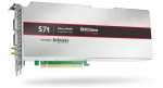
I wrote about Cadence AI IP not long ago when I covered the Cadence Automotive Summit at the end of July (Tensilica DNA 100 Brings the AI Inference Solution for Level 2 ADAS ECUs and Level 4 Autonomous Driving, Tensilica HiFi DSPs for What I Want to Hear, and What I Don’t Want to Hear). One of those two blogs remains one of my most widely read blogs. In those blogs I spoke quite a bit about the Tensilica DNA 100 processor. Since that event was targeting automotive topics, the focus was of course on delivering advanced automotive features, such as ADAS. At the Linley Processor Conferences, the context is different as the emphasis is on processors. So rather than simply just talking about what is needed for automotive features, Cadence went deeper into the system architecture options that are delivering these solutions using DNA 100, which can apply to far more than automotive. Lazaar Louis, Cadence’s Senior Director of Product Management, Marketing and Business Development for Tensilica IP, did a great job as a presenter, including a short Q&A session.

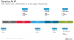
For AI edge inference, Cadence has three different types of processor IP. Users can choose the best solution for the specific workflow they are planning to use for each problem. This approach makes sense in automotive, where there are many different subsystems. It also makes sense when simply building a consumer IoT product where you want the correct processor for your price point and power budget. The Tensilica HiFi DSP product line is for audio, voice, speech, and AI applications. The Tensilica Vision DSP product line (including the recent Vision Q7 DSP) is for embedded vision processing, imaging, and AI. This year Cadence released the Tensilica DNA 100 as a standalone AI processor. With the increase in AI processing in consumer and automotive products, customers are implementing multi-core solutions with HiFi, Vision and DNA processor IPs to serve audio, vision and AI applications.

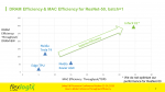
I cannot get into all the technical breadth of the Cadence-Linley presentation in this blog. If you want to see architectural details, I believe you can request a copy of the presentation through the Linley website, or simply contact your Cadence sales rep for more information. Lazaar’s presentation featured lots of details related to sparse computing, using a specialized neural network (NN) engine, scalability, high MAC utilization, using the Tensilica Neural Network Compiler, neural network libraries, minimizing accuracy loss due to quantization, and even more. It is rich and in-depth.

What I do want to remind you about is the need for a significant ecosystem. Software plays a large role in all AI/ML solutions. Beyond that you may need different types of semiconductor IP. Cadence is also part of Glow, Facebook’s community-driven approach to AI. Glow is a machine learning compiler for heterogeneous hardware. Cadence has committed to offering processor IP supporting Glow.

In August, I had focused more on the ecosystem around audio solutions as part of Cadence’s infotainment solutions. The list of partners in the embedded vision space is also impressive. Cadence highlighted eight of those partners at the conference, ArcSoft, MulticoreWare, Seemmo, Sensory, Visidon, Morpho, Almalence, and Irida Labs. These solutions can all be combined with Tensilica IP to make some truly amazing results.

Cadence is certainly “focused” (pun intended) on embedded vision. Cadence gave three presentations at the 2019 Embedded Vision Conference: Frank Brill, Portable Performance via the OpenVX Computer Vision Library: Case Studies; Pulin Desai, Highly Efficient, Scalable Vision and AI Processors IP for the Edge; and Shrinivas Gadkari, Fundamentals of Monocular SLAM. It will be interesting to see how cadence continues its effort in embedded vision in 2020.

On a final note, the Tensilica team has been supporting automotive standards for a long time. Rest assured that they have a handle on ISO 26262, ASIL levels, and everything related to automotive safety and reliability. What I pointed to in August, saw again at the AI Hardware Summit in September, at ARM TechCon in October, and at every technical conference I attend, there is one prevailing thought about AI/ML systems – “There is no safety without security.” Cadence’s partnership with Green Hills in this area is to be commended. Security will keep all this dream technology functioning without interference.

This is my final blog of three blogs from the Linley Fall Processor Conference for 2019. The first two blogs are here and here. If processors are your thing, or you just like staying current on the topic, you should consider going to the spring conference. Details are not yet announced, but you should be able to find them here once they are available.


KLAC- Very Strong Sept & Guide-Foundry up 50%- 5NM & EUV drivers- Outperforming

KLAC- Very Strong Sept & Guide-Foundry up 50%- 5NM & EUV drivers- Outperforming
by Robert Maire on 11-05-2019 at 6:00 am

  • KLAC Strong Beat on Both Sept Q & Dec Guide
  • Foundry/logic (TSMC) up 50% H2 vs H1
  • Gen 5 acceptance and 5NM rollout drive future

Strong beat in Sept results and Dec Guide
KLAC reported revenue of $1.41B and EPS of $2.48 handily beating street estimates of $1.5B and $2.20 in EPS. More importantly the company guided December to be revenues between $1.425B to $1.515B ($1.475B midpoint) and EPS between $2.39 and $2.69 ($2.54 midpoint), substantially higher than street estimates of $1.39B and $2.35.

The company also upped its estimate of WFE spend in calendar 2019 as the second half of the year has obviously turned out way better than the first half.

Foundry/Logic up 50% H2 versus H1
As we had suggested in our preview, the biggest uptick in business is Foundry/logic which is primarily TSMC spending a lot of money. Even Intel doesn’t come close. Memory remains weak and shrinking versus foundry/logic as a percentage of KLA’s business.

KLA’s core remains very strong
The orbotech acquisition hid the strength of the core KLA business which was up 16% sequentially while the Orbotech business was down slightly for a total 12% sequential growth which in our view is very strong considering that memory is still soft. Obviously this is a very strong annualized rate.

Reticle Inspection outperforming
Wafer inspection was up 13% sequentially but “patterning ” (reticle inspection) was up a whopping 31% sequentially which we attribute to some competitive wins mainly against Japanese competition.

Taiwan (TSMC) led the way with 27% of business with China at 24% , Korea (memory) a low 14% …even Japan was bigger at 15%, US was 13% (Intel).

2020 should be a very good year
The spend by TSMC on 5NM looks to be very large going into 2020. One reason we would cite is that there is little to no equipment reuse from 7NM to 5NM that we expect, so spending on 5NM by TSMC and 7NM by Intel will be for a lot of new equipment. We would also expect some sort of at least partial pick up in memory some time in 2020.

EUV transition pays dividends to KLA
As TSMC transitions from a few layers using EUV to most critical layers using EUV we will not only see a significant jump in EUV scanners, which obviously benefits ASML, but also a corresponding increase in KLA tools to support EUV.

This 4X to 5X increase in the number of EUV layers requires a lot of tools.
Intel, which has not put EUV into production will transition to EUV and will follow a similar tool and spending path as TSMC before it.

Industry Outperform
As we had previewed, its clear that KLA will outperform the growth of the overall semi equipment industry as they have historically been most closely tied to the fortunes of Foundry/Logic which is clearly as strong as memory was two years ago, perhaps even more so.

We think that Foundry/Logic leads memory spending over the next 3 to 4 quarters at least, as we still don’t have a solid idea as to the timing of a memory recovery. This suggests that KLA should keep up the industry outperforman as well given its tie to Foundry/Logic.

The Stock
We would continue to be a buyer of KLAC given the strong report coupled with excellent financials and value returns to shareholders which form a complete picture of an attractive value. Dividends and returns to shareholders continue their 15% trajectory with strong free cash flow and gross margins which continue to lead the industry by a very wide margin. We would view KLAC as our top large cap pick in the space.


Achronix Announces New Accelerator Card at Linley Fall Processor Conference – VectorPath

Achronix Announces New Accelerator Card at Linley Fall Processor Conference – VectorPath
by Randy Smith on 11-04-2019 at 10:00 am

This blog is my second blog from this year’s Linley Fall Processor Conference. The first two blogs focused on edge inference solutions. Achronix’s discussion was much broader than just AI/ML; it was about where FPGA’s have been going and culminated with a product announcement preview. I’ll get to the announcement in a moment, but first, let’s review the growth in FPGA and the markets it serves based on what Manoj Roge, Achronix VP of Product Planning & Business Development presented at the conference.

FPGA 1.0 was the first broad adoption of FPGA technology. The largest usage of FPGA technology was initially in “glue logic,” which is logic used to integrated various components into a system, last-minute adjustments to systems, and programmable IOs. The usage of FPGA technology grew dramatically from the mid-1990s until around 2017. FPGA 2.0 supported more complex functions than FPGA 1.0. For example, in EDA, we saw the growing use of FPGAs in prototyping, verification, and emulation. From FPGA 1.0 to 2.0, TAM (Total Available Market) grew from about $1B to $5B. But now FPGA technology is exploding as the number of growth areas is picking up dramatically. In the past year we have seen FPGA technology projected as an important piece of solutions in several areas including, data centers, edge compute, 5G infrastructure, and automotive, especially ADAS. Manoj implied we could see up to a 6x growth in FPGA TAM between 2018 and 2024.

Achronix is has been furthering the growth in FPGA usage by making the technology available in multiple forms. Achronix has made its FPGA technology available in chip form (Speedster7t), as IP for use as embedded FPGA (called eFPGA) in its Speedcore and as chiplets with its Speedchip FPGA Chiplets. That is many ways to access some very high-performance FPGA technology. Achronix didn’t simply rely on PPA (performance, power, and area) benefits of 7nm FinFET technology, but took a clean slate approach and did a grounds-up design to address the bottlenecks of traditional FPGAs. With Speedster7t, Achronix has reinvented high-performance FPGAs with three key pillars of architecture optimizations – making the compute efficient for Machine Learning Inference, designing the right memory hierarchy, and bandwidth and by efficiently transferring data between compute and memory through true two-dimensional Network on Chip (NoC).

At the conference, Achronix also mentioned VectorPath. This information was a bit surprising since VectorPath was not yet formally announced, but the press release did pop on October 29, 2019. The VectorPath™ S7t-VG6 accelerator card was part of a joint project between Achronix and BittWare, a Molex company. The VectorPath accelerator card will deliver high-performance and high bandwidth at dizzying levels for an FPGA. Pricing was not mentioned, but availability is expected at the beginning of Q2 2020. Features include:

  • 400GbE QSFP-DD and 200GbE QSFP56 interfaces
  • Eight banks of GDDR6 memory delivering 4 Tbps aggregate bandwidth
  • One bank of DDR4 running at 2666MHz with ECC
  • PCIe compliance and certification
  • 20 Tbps 2D NoC inside the Speedster7t FPGA
  • 692K 6-input LUTs
  • 40K Int8 MACs that deliver >80 TOPs
  • OCuLink – 4-lane PCIe Gen 4 connector for connecting expansion cards

There are some interesting choices here. The high-speed interfaces are what data centers are looking for now as they moved forward with 400GbE deployments. Card features have been thought through well so that enterprise-class customers can deploy confidently and future proof their designs with lot of application flexibility. It has been designed for both evaluation and high-volume production applications with the ability to even get this pre-integrated into a Dell or HPE server platform, speeding time to market.

Both GDDR and DDR4 are included, though I think it is the availability of GDDR6 memory support that is critical for highest-speed applications. As you see above, there is even more, but I am sure you get the point that this is seriously fast.

The Speedster7t FPGA family features a 2D network-on-chip (NoC) with more than 20 Tbps bandwidth capacity to efficiently move the data within the FPGA fabric and between the highspeed IOs and the FPGA fabric. The NoC supports AXI channels, so you are still using an industry-standard interface.

To use an FPGA, you need design tools. All the Achronix products mentioned above can be programmed using the ACE  design software, which is included with the purchase of a VectorPath card. ACE handles IP configuration, place & route, timing analysis, bitstream generation/download, and in-system debugging. The synthesis technology is Synplify-Pro from Synopsys though you get it through Achronix. The VectorPath product also comes with a comprehensive board management controller, OS support (Linux or Windows), API, drivers, application examples, and diagnostic self-test. The ability to use the same FPGA code (RTL) and tools across all these FPGA products is a nice feature to have. You could develop code on an accelerator card, reuse parts of it in chiplets, or elsewhere – truly reusable IP, and it is your IP.

I have one more blog coming from the Linley Fall Processor Conference for 2019. If you are into processors, you should consider going to the spring conference. I don’t think the details are announced yet, but you should be able to find them here once they are available. The leading edge is showing up at this event.


Intel CEO Update Q4 2019

Intel CEO Update Q4 2019
by Daniel Nenni on 11-04-2019 at 6:00 am

Bob Swan started as interim CEO in June of 2018 and took the full-time CEO job in January of 2019. I was a vocal critic of the previous CEO Brian Krzanich (BK) and really felt he was not fit to serve. As it turns out I was right. It is not just the CEO himself, but also the people that he surrounds himself with. BK surrounded himself with the Intel old guard and a couple of questionable newcomers, the rest is history.

I do have to thank BK as he is one of the reasons why I am somewhat famous or infamous. We had a very public feud back in the dark days of Intel 14nm and 10nm.

While I am not a fan of CFOs (followers) who become CEOs (leaders) I have high hopes for Bob Swan and the people with whom he will surround himself.

If you take a look at the Intel executive staff today there have been quite a few changes, most notably the addition of Jim Keller as senior vice president in the Technology, Systems Architecture and Client Group (TSCG) and general manager of the Silicon Engineering Group (SEG). Jim is responsible for “architecting the silicon engineering organization within TSCG”. This is a seriously disruptive move on the part of Intel.

For those of you who have not heard of Jim here is his career path graphic:

Jim is mentioned in our book “Mobile Unleashed” in the Apple chapter by the way. PA SEMI figured prominently in the success of the Apple SoC efforts. Jim really is a Silicon Valley legend amongst us semiconductor soldiers in the SoC trenches.

To get a better understanding of Jim Keller take a look at his recent Youtube video he did entitled Jim Keller: Moore’s Law is Not Dead:

It is a full hour but well worth your time, especially if you are one of the ill-informed who think Moore’s Law is dead.

Back to Bob Swan and 10nm, 7nm, 5nm, and 3nm. In the recent conference call Bob mentioned that Intel will get back to the Tick-Tock two year cadence where Tick is a new process and Tock is a new product architecture. Here are some cut/pasted comments from Bob:

The Intel 10-nanometer product era has begun and our new 10th Gen Core Ice Lake processors are leading the way. In Q3, we also shipped our first 10-nanometer Agilex FPGAs. And in 2020, we’ll continue to expand our 10-nanometer portfolio with exciting new products including an AI Inference Accelerator, 5G base station SoC, Xeon CPUs for server storage and network and a discrete GPU. This quarter we’ve achieved power on exit for our first discrete GPU DG1 an important milestone.

We are on track to launch our first 7-nanometer based products, a data center focused discrete GPU in 2021 two years after the launch of 10-nanometer. We are also well down the engineering path on 5-nanometer.

Back in our Analyst Day, we tried to go through this in quite a bit of detail, both, one, kind of our lessons learned coming out of the challenges we had with 10 and how we’re capturing those lessons learned as we think about the next two generations. But first our focus and energy is right now around scaling 10.

And, as we said, we feel very good about the capacity we put in place, the products we have coming down the pipeline and the yields that we’re achieving, almost week-on-week improvement over the last six months. So for 10, we feel really good.

Second, when we put the design rules in for 7-nanometer, we were less aggressive in terms of density. Our learning from going from 14 to 10 is with a benefit of hindsight, we were just — we tried to scale at a 2.7 factor and that was — that ended up putting too much invention or revolutionary nodes into the fab environment to meet those kind of hurdles and the learning from that is, we just can’t hit those kind of really aggressive targets, when, to your point, the dynamics are getting increasingly challenging. So lots of learnings out of 10. Our transition to 10 that we incorporated into 7, the design the design rules there’s less complexity and for the last couple of years that we’ve been working with EUV.

Litho has been the challenge. We’ve had EUV that we’ve been working with for a few years now and we expect to use EUV as we scale 7. And we indicated that our first product will be two years from this quarter. So fourth quarter of 2021, our first 7-nanometer product will come out and our expectation is that we’ll get back on a two-year cadence from 7 and beyond. So lots of learning out of 10-nanometer that we’ve incorporated, and we said back in May and we reiterated today, we expect to be back to a two to two-and-a-half year cadence going forward at least for the next few nodes.

Bottom Line: Intel got too aggressive at 10nm with 2.7x scaling without EUV and the design rules were much too complex for the process maturity. Intel 10nm is finally in HVM after a four year delay and 7nm is well under way. EUV is in HVM at TSMC, TSMC did the heavy EUV lifting, so I have confidence Intel will get 7nm in 2H 2021, hopefully.

Intel 7nm will be FinFETs (yawn) but Intel 5nm will be horizontal nanosheets and Intel 3nm CFETs. Interesting times ahead at Intel, absolutely!

Related Blog


Shipments of 5G Smartphones Will Surge to 900 Million Units in 2024

Shipments of 5G Smartphones Will Surge to 900 Million Units in 2024
by Robert Castellano on 11-03-2019 at 6:00 am

5G smartphones will increase from just 13 million units in 2019 to 900 million in 2024, as previous 2G/3G/4G smartphones shipments will decline slightly over the 2019-2024 period, reaching parity with 5G smartphones in 3Q 2023, as shown in the chart below.

According to The Information Network’s report “Hot ICs: A Market Analysis of Artificial Intelligence, 5G, CMOS Image Sensors, and Memory Chips,” 5G smartphones will surge at a CAGR of 130% during this period,. 2G/3G/4G smartphones will exhibit a CAGR of -10%, as their share of the overall smartphone market drops from 99% in 2019 to 48% in 2024.

In addition to the technical benefits of 5G, which are designed to transfer data 10 to 100 times faster than current 4G technology, prices will also drop significantly during this timeframe. In 2019, 5G phones are selling for twice that of 2G/3G/4G. But in 2024, 5G smartphone prices will have only a 10% premium over older phones.


VW Drops Connected Car Bombshell

VW Drops Connected Car Bombshell
by Roger C. Lanctot on 11-03-2019 at 6:00 am

A senior executive from Volkswagen North America kicked off Enterprise Ireland’s first annual “CASE: Driving the Future” mobility symposium last week with the announcement of the launch of its next generation Car-Net connected car platform. The new solution represents a breakthrough by allowing for the customer selection of preferred wireless carrier and the ability to add a new connected VW to an existing consumer wireless plan.

The VW announcement was a bombshell not only for this novel multiple-carrier configuration but also for the fact that it marks Verizon Wireless’ return to the connected car market six years after General Motors’ OnStar service opted for AT&T Mobility over Verizon. The VW announcement is something of a poke at AT&T as well, which is VW’s existing connectivity provider.  AT&T may yet be added to the new Car-Net platform in 2020 as a customer option.

The new Car-Net system also marks a change in business model for VW – offering new car customers five years of free remote access functionality (remote start, remote lock/unlock) from the company’s mobile app with OnStar-like automatic crash notification via the on-board modem as a $99/year add-on. The Car-Net service was previously offered as a complete package at $199/year.

New cars with the updated Car-Net service will start arriving soon in the U.S. – with a line-wide upgrade expected to be completed during the course of 2020. Verizon is the first carrier enabled on the Car-Net platform thanks to software and service provided by Ireland-based supplier Cubic Telecom. (Cubic Telecom investors include Volkswagen’s Audi division, Qualcomm, and eSIM supplier Valid.) T-Mobile is expected to be added soon to Car-Net via remote provisioning of the on-board e-SIM by Cubic. Volkswagen also expects AT&T to be an option in the future.

The announcement opens a new chapter in vehicle connectivity – one in which consumers can tap a re-provisionable connectivity device in a connected car in order to simply add their car to their existing wireless plan. The new connectivity means cars may actually come to be seen by consumers as smartphones on wheels.

VW intends to use the new platform to deliver streaming services, usage-based insurance, vehicle diagnostics and service scheduling, and integrated e-commerce capabilities for paying for parking, tolls, and fuel. All of the richness of the VW/Cubic value proposition will be realized in due time. The announcement shows VW stealing the connectivity innovation flag from Detroit’s GM and planting it firmly in Herndon, Va., VW NA’s headquarters. The multiple-carrier solution and device add-on functionality is only currently enabled in the U.S. and Canada largely due to regional regulatory limitations elsewhere in the world.

Related Blog


AMD Intel TSMC menage a trois and the trouble with trouples

AMD Intel TSMC menage a trois and the trouble with trouples
by Robert Maire on 11-01-2019 at 10:00 am

  • Its “Complicated”- A 3 way Chip Relationship
  • Competing for Wafers, Moore’s Law & Love
  • Who’s Competing with Whom?
  • All’s Fair

The 3 way relationship is more complex than it seems

On the surface it seems simple. AMD and TSMC compete with Intel making its own chips and TSMC making them for AMD. But below the surface the real competition is actually between Intel and TSMC for supremacy in Moore’s Law as that will determine chip performance, value and cost. Maybe not…Dig down another layer and maybe its a competition between the US and a foreign competitor. Dig a little deeper and its a clash of China versus the US.

So the competition is AMD  & China Versus Intel? Or is it? Could it be Intel & AMD versus TSMC? Could it be Intel & TSMC versus AMD? Maybe all three.

Falling down the rabbit hole

Everything seems simple until you ask who TSMC’s biggest customers are. You might answer with the obvious choices. Apple, Huawei, Qualcomm, AMD and who else? You might answer Nvidia or HiSilicon, Marvell, Broadcom, Mediatek as number 5 but what if Intel was a top customer of TSMC? Well that strange revelation may actually be the case TSMC has been making chips for Intel and Intel has been short of capacity.  Intel may be freeing up some capacity by off loading production to TSMC maybe a lot maybe a lot more.

A secret, convenient, affair?

Its not like either Intel or TSMC would want the “relationship” publicized. AMD might get mad at TSMC cheating behind their back and Intel might be embarrassed that it would have to go to its erstwhile competitor to get needed capacity…. much better to keep the “side” relationship quiet and discrete.

Is Intel really serious about Competing with TSMC?

Is Intel actually reducing “leading edge” capex?

On Intel’s recent conference call they spoke about wanting to get back on a 2 or 2.5 year Moore’s Law cadence after stumbling around for 5 years with the 14/10NM transition. Sounds good but they may not be putting their money where their mouth is?

Intel announced a $500M increase in Capex which sounds like a lot of money but in the scheme of things is really just a bit over 3% increase from their current Capex budget, a fairly paltry increase. More importantly Intel said on their call that a significant portion of their Capex was going to increase capacity.  We would interpret this “significant” capacity increase at likely more than 3% of their capex spend. The capacity increase is aimed more at 14NM and other non-leading edge geometries so the spend is not aimed at pushing Moore’s Law rather just making more of the same parts.

This suggests that the math means that actual Capex spend on 5NM and 7NM , leading edge, may actually be down after you take out the capacity spend.

This hardly seems like a way for Intel to get back on a 2 to 2.5 year Moore’s Law cadence let alone catch up to TSMC which had a huge (much bigger than 3%) increase in their capex.

So this begs the question if Intel is truly serious about catching TSMC… The numbers would indicate not… Maybe Intel really doesn’t want to compete…

Could Intel go “fab lite”? Shades of “real men have fabs” and Jerry Sanders at AMD

Maybe the financial math would be better for Intel to go fabless and throw its manufacturing to TSMC.  Its clearly working better than what they have done lately, Works for Apple. Has gotten AMD back in the race.

Maybe like Apple, AMD, Qualcomm and others you do the design and keep the IP and hand the dirty and capital intensive work to TSMC.

It would be funny to have both AMD and Intel CPUs made by TSMC….not a lot different from Apple and Huawei both getting their chips made by TSMC or Qualcomm and Broadcom or MediaTek and Marvell….. seems to be the model….

It begs the question that has been asked many times…why does Intel still have fabs?

Everybody is competing for TSMC’s love and capacity

People might say that Intel would never put itself in a position where it had to compete for capacity at TSMC versus AMD but the truth is that Intel is already there…just not at bleeding edge CPUs.  Apple is obviously TSMC’s favorite… Qualcomm always wants to keep a relationship with Samsung to keep TSMC honest and get more capacity.

Its like a bunch of teenagers fighting over who loves who more.  In this case, TSMC may be the object of everyone’s desire.

More plot twists & strange relationships than an opera

There are a lot of moving parts in these strange relationships. TSMC is a “frenemy” to Intel, Samsung is a “frenemy” to Apple.  All these are small sub-plots against the giant overarching drama between the US and China which desperately wants to take over both Taiwan and the Chip industry and they are both one and the same.  The trade war is a backdrop to the overarching drama.

Could Apple turn it into a four way drama?

What if Apple decides to dump Intel and X86 in favor of its own processors, for laptops and desktops, made by TSMC. Or could Apple go in the opposite direction and ask Intel to make its custom processors in Intel fabs in order to stamp them “Made in America” and avoid the China take over and IP risk? (not likely…but stranger things have happened..)

The risk factor in making almost every significant chip on the planet (other than Intel) on a small island an hour and a half sail away from China by one company seems strange when you think about it.

The stocks

Right now the drama continues to play out without a lot of definitive conclusions. We need to monitor Intel’s progress in both capacity and Moore’s Law and see if they can get it together.  Can AMD get the attention and capacity it needs form TSMC? Will Intel increase or decrease business with TSMC? What will happen with the trade war? When and how will Samsung come back? Will they give up on being a foundry?

Right now the best positioned company appears to be TSMC which sits at the nexus of the drama and is the friend that everyone wants to have which an enviable place to be. Intel is in wait and see mode and AMD has potential but needs to execute.


Samsung 2019 Technology Day Recap!

Samsung 2019 Technology Day Recap!
by Daniel Nenni on 11-01-2019 at 6:00 am

Samsung is a complicated company with a VERY long history. We attempted to capture the Samsung Experience in chapter 8 of our book “Mobile Unleashed: The Origin and Evolution of ARM Processors In Our Devices”. If you are a registered SemiWiki member you can download a free PDF copy in our Books section.

Here is the chapter 8 introduction:

To Seoul, via Austin

Conglomerates are the antithesis of focus, and Samsung is the quintessential chaebol. From humble beginnings in 1938 as a food exporter, Samsung endured the turmoil and aftermath of two major wars while diversifying and expanding. Its early businesses included sugar refining, construction, textiles, insurance, retail, and other lines mostly under the Cheil and Samsung names.

Today, Samsung is a global leader in semiconductors, solid-state drives, mobile devices, computers, TVs, Blu-ray players, audio components, major home appliances, and more. Hardly an overnight success in technology, Samsung went years before discovering the virtues of quality, design, and innovation. The road from follower to leader was long and rocky.

And here are the final thoughts of the chapter:

A bigger question is how Samsung, and others, continue to innovate in smartphones beyond just more advanced SoCs. There are also other areas of growth, such as smartwatches and the IoT, where Samsung is determined to play. There are me-too features, such as Samsung Pay, and new ideas like wireless charging and curved displays. (More ahead in Chapter 10.)

How this unfolds, with Samsung both supplier and competitor in an era of consolidation for the mobile and semiconductor industries, depends on adapting the strategy. Innovations in RF, battery, and display technology will be highly sought after. Software capability is already taking on much more importance. As Chinese firms improve their SoC capability, the foundry business may undergo dramatic changes – and the center of influence may shift again.

 History says Samsung invests in semiconductor fab technology and capacity during down cycles preparing for the next upturn. Heavy investments in 3D V-NAND flash, the SoC foundry business, and advanced processes such as 10nm FinFET and beyond are likely to accelerate, and competition with TSMC and other foundries will intensify as fab expenses climb.

This book was published in December of 2015 and while there have been lots of changes at Samsung many things remain the same. Remember, they have the full support of South Korea including the government and more than 51 million people.

Bottom line: Samsung is a brute force technology innovator and we are very lucky to have them as a leader in the semiconductor industry, absolutely!

The Samsung Technology Day featured three key announcements introduced by the president of Samsung Semiconductor:

“Samsung is focused on harnessing the most advanced semiconductor technologies to power innovation across key markets,” said JS Choi, president, Samsung Semiconductor. “From System LSI devices that are perfectly adapted for real-world 5G and AI, to advanced solid-state drives (SSDs) that handle mission-critical tasks and offload CPU workload, we are determined to deliver infrastructure capabilities that are built to enable every wave of innovation.”

  • Exynos 990 and 5G Exynos Modem 5123:Delivers unprecedented AI-powered user experiences on-device with a dual-core neural processing unit (NPU) and enhanced digital signal processor (DSP) that can perform over ten-trillion operations per second. The Exynos 990 and 5G Exynos Modem 5123 harness the most advanced chipmaking technologies to-date with a 7-nanometer (nm) process using extreme ultraviolet (EUV) lithography.
  • Third-generation 10nm-class (1z-nm) DRAM:Delivers the industry’s highest performance, energy efficiency and capacity, since mass production in September. Optimized for premium server platform development, the 1z-nm DRAM will open the door to a lineup of memory solutions at the cutting-edge such as DDR5, LPDDR5, HBM2E and GDDR6 products as early as the beginning of next year.
  • 12GB LPDDR4X uMCP (UFS-based multichip package): Combines four 24Gb LPDDR4X chips and an ultra-fast eUFS 3.0 NAND storage into a single package, breaking through the current 8GB package limit in mid-range smartphones and bringing more than 10GB of memory to the broader smartphone market.

Personally, I found the event well organized and the presentations very well done. They were personalized and entertaining. One of the comments was that Samsung will dramatically increase their cloud silicon business. Currently they have 0% market share so the sky is the limit, literally.


BittWare PCIe server card employs high throughput AI/ML optimized 7nm FPGA

BittWare PCIe server card employs high throughput AI/ML optimized 7nm FPGA
by Tom Simon on 10-31-2019 at 6:00 am

Back in May I wrote an article on the new Speedster7t from Achronix. This chip brings together Network on Chip (NoC) interconnect, high speed Ethernet and memory connections, and processing elements optimized for AI/ML. Speedster7t is a very exciting new FPGA that can be used effectively to accelerate a wide range of processing tasks. Naturally with an announcement like this, the question of how to deploy this chip arises. Not everyone who could benefit from this new technology has the skills, time or resources to build it into a system. Data center operators who want to deploy this chip need a ready-to-go accelerator to make this happen.

Fortunately, Achronix just announced a major design win for their Speedster7t that will help end users get this chip into their server farms and data centers. Achronix and BittWare, a subsidiary of Molex, have teamed up to produce the VectorPath S7t-VG6 Accelerator Card. With it there is now an enterprise class PCIe accelerator card that can be used to provide best in class FPGA acceleration for cloud and edge computing.

The trend of adding data center accelerators has been heating up recently and the annual market is estimated to be around $2.8B for 2019. Forecasts have this growing to around $21B by 2023. Of this, the FPGA accelerator segment should be the fastest growing with a size of over $5B by 2023. This is because FPGA based accelerators hit on every cylinder when it comes to meeting business and technical needs.

FPGA accelerators offer very high performance per watt for a number of applications. Because they are reconfigurable, they allow the agility to take advantage of new algorithms or to be adapted for new applications. Because the BittWare VectorPath S7t-VG6 uses PCIe, it is easily scalable with the addition of any number of needed cards. Deployment is made easy with a full suite of development tools and BittWare’s support resources.

The VectorPath S7t-VG6 is a full height ¾ length (GPU size) double wide card with passive, active or liquid cooling options. The on-board hardware is well thought out. There is 8GB of 4Tbps GDDR6 as well as 4GB of DDR4. The PCIe interface is Gen3 x16. The card is expected to support Gen4 with qualification. The Ethernet interfaces use hard MAC and FEC IP that support a wide range of standard protocols and line rates. There is a 1x 400GbE interface that can be configured as 2x 200, 4x 100, or 8x 10/25/40/50GbE. There is also a 1x 200BgE interface that can be configured as 2x 100 or 4x 10/25/40/50GbE

To make the card even more useful there are clock and interface expansion options. On the front of the card there are clock inputs for 1PPS + 10MHz. On the back there are 3.3V GPIOs that are useful for control, triggers and adding support for legacy interfaces. Additionally, on the back there is an OCuLink expansion port that adds a lot of flexibility. It can be used for PCIe Gen4 or for general purpose SerDes. It offers low latency card-to-card connections for deterministic scaling. Or, it can be used at add extra network ports, add NVMe FLASH, or to define custom serial I/O interfaces.

The news release from Achronix and BittWare has a lot more information about customization options, developer’s toolkit and goes into more depth on the advantages of the Speedster7t FPGA. One of the key take-aways is that BittWare has the resources and technology to make deployment of the S7t VG6 accelerator card practical for a wide range of end users. I suggest looking at the full release on their websites to get more information.


Efficiency – Flex Logix’s Update on InferX™ X1 Edge Inference Co-Processor

Efficiency – Flex Logix’s Update on InferX™ X1 Edge Inference Co-Processor
by Randy Smith on 10-30-2019 at 10:00 am

Last week I attended the Linley Fall Processor Conference held in Santa Clara, CA. This blog is the first of three blogs I will be writing based on things I saw and heard at the event.

In April, Flex Logix announced its InferX X1 edge inference co-processor. At that time, Flex Logix announced that the IP would be available and that a chip, InferX X1, would tape out in Q3 2019. Speaking at the fall conference, Cheng Wang, Co-founder and Senior VP of Engineering, announced that indeed, the chip did tape out in Q3. Also, Cheng said that first silicon/boards would be available sometime in March 2020, there would be a public demo in April 2020 (perhaps at the next Linley Conference?), and that mass production will be in 2H 2020. While this means that Flex Logix is delivering on the announced schedule, there was certainly a specific focus to Cheng’s presentation beyond that message. In a word – Efficiency.

In engineering fields, we often compare different efforts or approaches to the same problems using benchmarks. When it comes to looking at finished products, these benchmarks can be straight-forward. For example, we review miles per gallon, acceleration, stopping distance, and other factors when analyzing the performance of a car. For processors, it has always been a bit more difficult to do benchmarking. I remember working with BDTi nearly 20 years ago when trying to compare the performance of various processors for video processing with widely different architectures. It took an organization like BDTi to give an unbiased analysis, though it was still challenging to see how the results related to your real-world needs.

There is an increasing number of processing options now being developed and deployed for neural network inference at the edge. More and more, we see attempts to standardize the benchmarks for these solutions. One example is Stanford University’s DAWNBench, a benchmark suite for end-to-end deep learning training and inference. But reading through this information, you still will come to realize that it is your specific application that truly matters. Why look at benchmark results for “93% accuracy”, if you must meet “97% accuracy”? Does Resnet 50 v1 accurately represent the model you will be running? In particular, DAWNbench was ranking results based on either cost or time. As engineers though we typically face criteria in a different manner – hard constraints and efficiency.

Hard constraints are easy to understand when looking at these benchmarks as there will be simple constraints for area, power, and performance. Likely, multiple architectures may be able to meet all or most of these constraints, though perhaps not simultaneously. But to understand which approach meets them best, you need to consider efficiency – inferences per $, and inferences per watt. This method of showing performance is where Flex Logix’s InferX X1 approach seems to separate itself from the competition, at least for the devices shown. From the Flex Logix presentation at the Fall Conference:

DRAM costs money, so it is important to be efficient in your use of DRAM. If you are not considering DRAM efficiency in making your selection of IP, then you are not measuring your true costs. The DRAM requirements to hit a certain performance level are not equal between the various processors.

The one thing that has been clear to me this year, especially having attended both the AI Hardware Summit and the Linley Fall Processor Conference, is that simply measuring TOPS is a waste of time. See below the information presented by Flex Logix on TOPS across a few well-known solutions. In this example, InferX X1 would seem to be a minimum of 2x more efficient than the Nvidia solutions.

The entire Linley Fall Processor Conference presentation from Flex Logix is available on their website here. It is not possible to share all the details in a blog here, but I encourage you to see the entire presentation. There is more information available in the presentation about how this efficiency is achieved and how to accurately predict inference performance (how Flex Logix confirmed their performance pre-silicon).