
The headline screams off of the page and challenges all that we know about the fatal crash in Tempe, Ariz., that took the life of Elaine Herzberg two and a half years ago. “Backup Driver of Autonomous Uber SUV Charged with Negligent Homicide in Arizona.”
How could the National Transportation Safety Board (NTSB) associate itself with such an outcome? Shouldn’t Uber ATG bear full responsibility for the crash?
An NPR (National Public Radio) report notes that “Rafaela Vasquez (the driver of the Uber Advanced Technologies Group car) appeared in court on Tuesday (last week) in Maricopa County, Ariz. She pleaded not guilty to the (negligent homicide) charge and has been released with an ankle monitor. Her trial is set for Feb. 21st.”
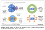
A glance at the extensive NTSB reporting on its investigation reveals a Volvo SUV kitted out with a vast sensor array including:
- A Velodyne Lidar
- Eight radar sensors
- Ten cameras
- 12 ultrasonic sensors
- GPS, Inertial Measurement Unit, and LTE
The report also details the decision-making protocols written into the software code defining the automated driving system (ADS) and further notes the vehicle was designed to operate only in designated areas that had been “mapped” by Uber. Not all sensors were operational and when the ADS system was engaged the existing advanced driver assistance system in the underlying Volvo SUV was disengaged.
NTSB Final Report on Uber ATG Crash: https://www.ntsb.gov/investigations/AccidentReports/Reports/HAR1903.pdf
Responsibility for the crash could be credibly attributed to Uber on a variety of levels including the configuration of the system, the reliability and robustness of the underlying software code and algorithms, the reliability of the hardware including sensors and processors, the quality of the underlying map governing the operational design domain (ODD), and the training of the “safety driver.”
Uber’s responsibility, no liability, virtually shouts from the pages of the NTSB report. In the instance of the fatal crash, for instance, the system determined that emergency braking was required, but the emergency braking maneuver is not enabled when the car is in self-driving mode, according to NTSB findings. Uber stated that this was intended to reduce the likelihood of erratic stops on public roads (something Tesla vehicles have been found to do). It was up to the safety driver to intervene – but the system was not designed to alert the driver when emergency braking is required.
It’s true that the safety driver was distracted at the time of the crash – watching a television program on a mobile device brought into the car. Video recorded by the vehicle’s driver monitoring system clearly reveals this distraction.
The purpose of the driver monitor is to ensure that the driver remains engaged in the driving task. Uber failed to link the driver monitor system to either a driver warning or to a disengagement of the automated driving system. The fatal crash is a strong argument for simultaneous remote driver monitoring if not remote vehicle control in such a testing circumstance.
Worse even than these issues, though, was Uber ATG’s history of crashes as reported by the NTSB:
“ATG shared records of fleet crash history with NTSB investigators. The records showed that between September 2016 and March 2018 (excluding the current crash), there were 37 crashes and incidents involving ATG test vehicles which at the time operated in autonomous mode. Most of these crashes involved another vehicle striking the ATG test vehicle—33 such incidents; 25 of them were rear-end crashes and in 8 crashes ATG test vehicle was side swiped by another vehicle.
“In only two incidents, the ATG test vehicles were the striking vehicles. In one incident, the ATG vehicle struck a bent bicycle lane bollard that partially occupied the ATG test vehicle’s lane of travel. In another incident, the vehicle operator took control of the vehicle to avoid a rapidly approaching oncoming vehicle that entered the ATG vehicle’s lane of travel; the vehicle operator steered away and struck a parked car. In the remaining two incidents, an ATG vehicle was damaged by a passing pedestrian while the vehicle was stopped.”
The history reported by Uber ATG to NTSB suggests a less than stellar performance by the ATG system on the road leading up to the fatal crash. It is perhaps no surprise that both Uber ATG and its newfound partner in automated driving at the time, Nvidia, stopped testing their automated driving systems in the wake of the crash.
The conclusion of the NTSB was that the ADS was sufficiently proficient to lull the safety driver into a false sense of security and that Uber failed to put adequate countermeasures in place to overcome that driver complacency. In the end, though, the NTSB determined the probable cause of the crash to be “the failure of the vehicle operator to monitor the driving environment and the operation of the automated driving system because she was visually distracted throughout the trip by her personal cell phone.”
Uber settled with Elaine Herzberg’s family almost immediately. Uber ATG has made multiple changes in its program and resumed testing since the crash. But the surfacing of criminal charges against the safety driver two and a half years after the incident raises questions regarding responsibility and liability in the automotive industry.
With decent legal representation, the Uber safety driver should be able to avoid serious sanction or jail time. Given the flawed configuration of the automated driving system and the failure to link the driver monitor to its operation clearly points to Uber’s responsibility.
Getting this right, properly assigning responsibility, is essential to the creation, deployment, and adoption of semi-autonomous systems such as Tesla Motors’ Autopilot beta and General Motors’ Super Cruise. Before deploying these systems we must know how, when, and whether they will work. There is no excuse for allowing the attention of drivers to stray during automated operation – if a system is really semi- and not fully autonomous.
It’s pretty clear from the NTSB report that the Uber ATG system should never have been on the road as configured. It was a crash waiting to happen. In the process, Uber cast the entire autonomous vehicle project and the related regulatory framework – or lack of one – in doubt.
We are left with the unresolved issue of how to regulate automated driving – even as testing continues to expand across the U.S. and commercial deployments commence. The lack of a regulatory or enforcement infrastructure is the enduring legacy of the incident.
We are left with self-certification – which clearly failed in the case of Uber ATG. Regulators and legislators are left holding the bag – which is full of inscrutable software code and algorithms.
Advocates for Federal AV legislation are arguing for widespread regulatory exemptions for AVs, and Federal priority over future AV regulations concerning vehicle design and performance parameters. In this case, perhaps a Federal framework might be a good start.
In the meantime, all AVs ought to be equipped with remote driver monitoring as well as remote control. It is clear that in the Tempe, Ariz., crash Uber ATG lost all plausible deniability. The system recorded the driver’s misbehavior without doing anything about it. That ought to be immediately corrected.

