RVN! 26 Banner revised (800 x 100 px) (600 x 100 px)

Using Machine Learning to Improve EDA Tool Flow Results

Using Machine Learning to Improve EDA Tool Flow Results
by Daniel Payne on 08-25-2021 at 10:00 am

gajski kuhn

Back in 2020 I first learned from Synopsys about how they had engineered a better way to do optimize layouts on digital designs by using machine learning techniques, instead of relying upon manual approaches. The product was named DSO.ai, standing for Design Space Optimization, and it produced a more optimal floor-plan in less time than a human could, saving many man-months of effort. The world’s leading Android-based smart phones is Samsung, and they’ve used DSO.ai to optimize the design of their Exynos chips. Last week I followed up by Zoom to hear from two experts at Synopsys about the next steps in using machine learning, Thomas Andersen, VP, AI and Machine Learning and Stelios Diamantidis, Sr Director, AI Solutions.

At the highest level it is said that software is eating the world, with all of the activity in AI, increases in video use, and the growing number of data centers. Recently we see that AI is eclipsing software, and that is driving engineers to create new kinds of compute to meet the challenges. Chip designs are now being optimized to run the most prominent apps.

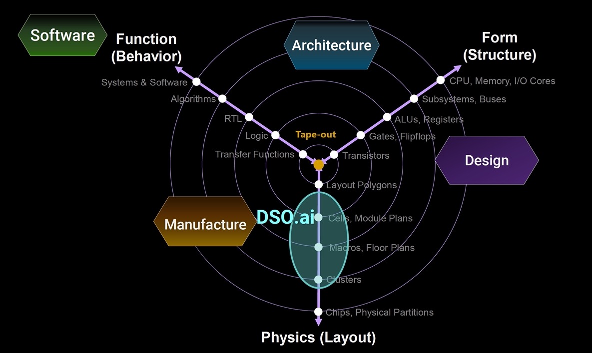
The first generation of DSO.ai could optimize a layout, then show you metrics like leakage power versus timing, allowing you to choose the best design. Shown below is the classic Y diagram, made famous by Gajski-Kuhn back in 1983. The area where DSO.ai works is shown highlighted in green:

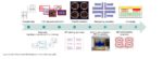
The optimizations within DSO.ai are controlled by an engineer setting multi-objectives and search spaces, then the tool runs using reinforcement learning and results are visualized in a plot. Systems companies like Google and NVIDIA have likewise done work in applying AI to their internal tool flow for macro placement of blocks, so this is a promising area to follow.

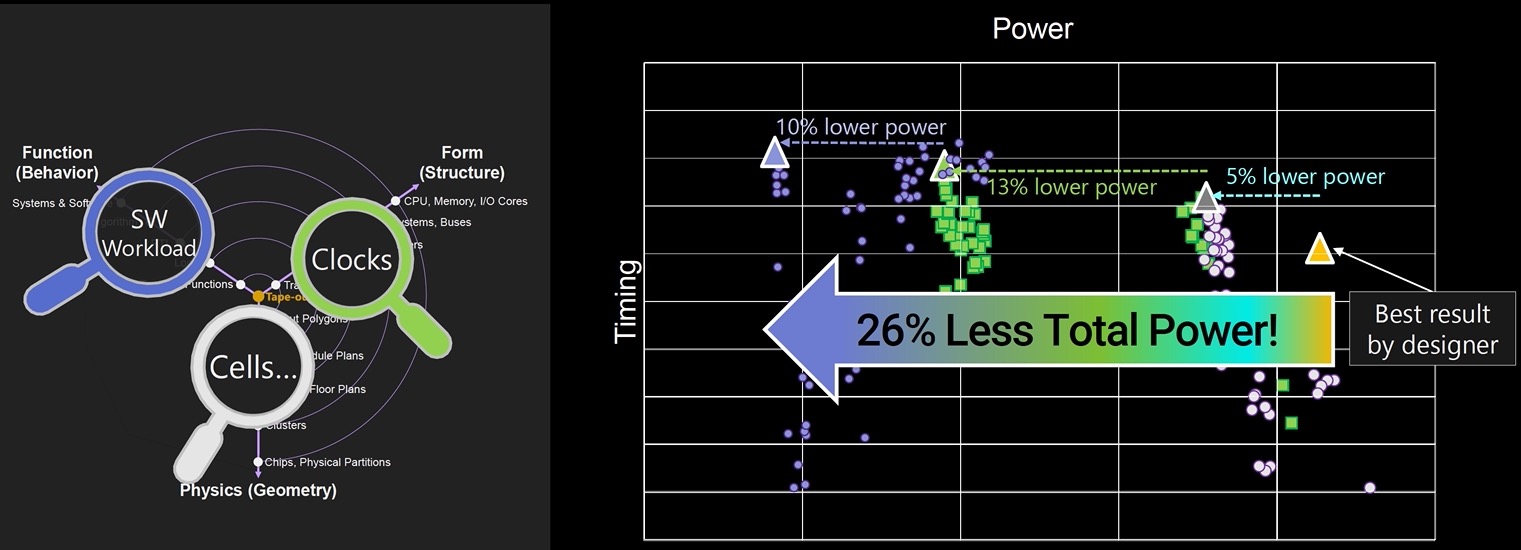
At the recent Hot Chips conference, Synopsys revealed that DSO.ai was now expanding beyond just optimizing layout, to optimizing clock gating and clock structuring in the RTL code. Furthermore, when you want to optimize for power, you can run your chip on an emulator as it executes an app, to drive the optimization. OK, so the concept sounds interesting, but where’s the data to prove the value?

An SoC design example was presented, where using just the layout optimizations showed a 5% power reduction versus a hand-crafted approach. Adding the clock optimizations by changing the RTL coding provided another 13% lower power number. Finally, using the actual power activity from running an app on the SoC through an emulator, the optimization achieved another 10% power reduction. Here’s the results:

I just needed to clarify that while these new optimizations in DSO.ai are on actual customer designs,  you’ll have to wait for any official product update announcement from Synopsys. The trend is clear though, engineers are going to enjoy less manual effort involved in the chip design process, because concepts like machine learning are suited to automate some of the tasks in the tool flow. Engineers still need to specify the constraints for the optimizations, and then build up on the a result, all while saving time in the process. Synopsys is the first EDA vendor to demonstrate the use of AI across all three axis: Behavior, Structure and Geometry.

I asked about the learning curve of DSO.ai, and was told that most teams are becoming productive within their first week. You will see the biggest benefits from using an all-Synopsys flow, although other vendor tools could be mixed in the flow, but the optimization engine doesn’t have as much ability to control a non-Synopsys tool. I wonder if other EDA vendors will want to get their point tools certified to be DSO.ai aware, in order to fit better into a Synopsys flow. Time will tell.

Each run with DSO.ai runs design tools, so iterating to create dozens of possible designs takes some time, however convergence is much faster compared to the manual approach. The concurrent optimization approach across behavior, structure and geometry is a bold idea.

Summary

No, we’re not at the point of AI designing new chips from scratch, even though that concept makes for a popular SciFi movie plot. Reinforcement learning has been successfully applied with the DSO.ai technology to optimize concurrently across three domains: behavior, structure and geometry. Early results look quite promising with this optimization approach.

Also Read:

How Hyperscalers Are Changing the Ethernet Landscape

On-the-Fly Code Checking Catches Bugs Earlier

Upcoming Virtual Event: Designing a Time Interleaved ADC for 5G V2X Automotive Applications


Expanding Intel’s Foundry Partnerships: A Critical Piece of IDM 2.0

Expanding Intel’s Foundry Partnerships: A Critical Piece of IDM 2.0
by Daniel Nenni on 08-25-2021 at 6:00 am

Stuart Pann SemiWiki

One of the career Intel employees (33+ years) that Pat Gelsinger brought back is Stuart Pann. Stuart is now the Senior Vice President of the Intel Corporate Planning Group. He does not have direct foundry experience but he certainly knows Intel and Pat so it will be interesting to see where this goes.

Stuart recently penned an article on Intel’s foundry partnership strategy that is worth a look. The audience for this seems to be Wall Street but I found it interesting due to the opening question and what was not discussed:

Significant elements of these graphics products will be manufactured externally, using TSMC’s N6 and N5 process technologies. This is the basis of a question I hear frequently in my role as leader of the newly formed Corporate Planning Group – where one of our jobs is to manage the relationships with our external foundry partners.

No mention of N3 usage at all? I was certainly hoping for a little more transparency here. The TSMC N3 wafer agreement is historical in nature due to its size and product scope.

But yes Intel’s tile (chiplet) strategy makes outsourcing much easier which is a brilliant move. The low cost Chiplet strategy will enable many new wafer starts for the semiconductor industry so you can bet this technology will move forward quickly, absolutely.

I’m asked: Why do we use foundries for products instead of our internal factory network and how do we make that decision?

The historical answer is “due to acquisitions”. The updated answer of course is “due to the Intel manufacturing delays”.

Intel has been using external foundries for decades. In fact, Intel currently runs as much as 20 percent of its overall product volume at external foundries, and we are among the top customers of TSMC. Historically we have partnered with foundries to manufacture components such as Wi-Fi modules and chipsets or specific product lines such as Ethernet controllers. These products use mainstream process nodes to complement our internal leading-edge technologies.

The 20% he mentioned comes from Intel acquisitions that were already using TSMC. Most of which have been moved to Intel internal manufacturing (Altera for example) but some have stayed. Given Intel’s new semiconductor consolidation push that 20% should grow inorganically as well as organically.

External foundries are strategic partners and a key component of our IDM 2.0 model. While the majority of our products will continue to be made internally, expect to see tiles from external foundries playing a bigger part in our modular products in the coming years – including core compute functionality on advanced nodes to serve emerging workloads in client, data center and other areas.

I’m sure this claim can be “unpacked” (Intel’s favorite new sound bite) and justified with a public relations spin but I see no possibility that the majority of die inside Intel finished chips will be manufacture by Intel once the TSMC N3 based CPU/GPU products reach HVM.  50.00001% is technically a majority but even then I find it hard to believe. TSMC is already at 20% without chiplets and the N3 contract.

Either way I’m looking forward to hearing more from Stuart.

On a side note, Intel branded their new GPU products ARC. Clever name certainly but it does cause confusion with the Synpsys ARC processors that were acquired from Virage Logic 10+ years ago. Synopsys has invested a lot of time and money in ARC technology so I highly doubt this will end nicely. But remember Intel is Synopsys’s biggest customer so it may all be handled quietly.

Also read:

TSMC Wafer Wars! Intel versus Apple!

Highlights of the “Intel Accelerated” Roadmap Presentation

Intel Accelerated


Symmetry Requirements Becoming More Important and Challenging

Symmetry Requirements Becoming More Important and Challenging
by Tom Simon on 08-24-2021 at 10:00 am

Symmetry across the design flow

Humans certainly have always had an aesthetic preference for symmetry. We also see symmetry showing up frequently in nature. The importance of symmetry in electronic designs has been apparent for decades. There are a host of analog structures that require balanced layout. For instance, these include differential pairs and current mirrors. Or sometimes sets of devices need to be matched for performance reasons. Even starting with a schematic clearly drawn to show the symmetrical relationship between elements among devices, there is no guarantee that the layout derived from it will possess similar symmetry. Siemens EDA has developed new features in their Calibre nmPlatform to help with these issues and several new symmetry issues that designers should mindful of. Sherif Hany at Siemens has written an informative white paper that covers these new features so that designers can see how symmetry verification can be added to their flows to help quickly find and fix them before tapeout.

Symmetry across the design flow

Even when correct by construction techniques are used to help implement symmetry, there are a lot of factors that can degrade the design. Despite common centroid placement, routing to devices can end up mismatched. Likewise, other factors such as dummy shielding devices, metal fill and DFM processing can adversely affect layout symmetry. Siemens has developed techniques that are context aware from a schematic perspective to ensure that symmetry is properly adhered to. Double patterning is another area where symmetry in a design can suffer. Calibre nmPlatform can help resolve this with symmetry-assisted color anchoring. The white paper offers an illustration of how this works.

When metal fill is added to meet chemical-mechanical-polishing requirements design symmetry can also be affected. Thus, both the original design and the filled design must be verified. It is now possible for some fill decks to incorporate symmetry checks to guide fill operations around sensitive metals.

The paper discusses the advantages even where designs are not at advanced nodes or designers may already have in-house developed checks in place. Sherif suggests that in house checks usually come with a fair amount of designer effort and are not necessarily comprehensive. Even though foundry rule decks do preliminary symmetry checks, extra checks can offer significant benefits. Siemens has implemented advanced checks that go far beyond the foundry supplied rule decks. These advanced checks can be extremely helpful in automotive applications, MEMS, silicon photonics or analog/RF.

Another concern that Sherif addresses in the white paper is how some verification solutuions are overly strict and report so many errors that the results are not useful. Apparently, there is such a thing as too accurate. Calibre implements a fuzzy symmetry capability that allows for tolerances by area or length to help make the results more useful. This can be especially useful for curvilinear structures that can have minor variations that are not significant.

There is also a discussion of the debugging features for the symmetry analysis. XOR results can be shown in the layout environment, which makes for easy debugging. Also results can be seen in Calibre RealTime tools. There is integration with Calibre PERC, using XML. Customization of the symmetry checks can easily be set up and modified to suit individual project needs.

The paper closes by asserting that, like other parts of the verification flow, symmetry checks are becoming more complicated and are increasingly necessary. Without a doubt designers will want to be able to fully check for symmetry issues before tapeout. It seems that Siemens is mindful of this and has taken a comprehensive approach to solving this challenge for designers. More information and the full white paper are available on the Siemens website.

Also Read:

Debugging Embedded Software on Veloce

SoC Vulnerabilities

A Custom Layout Environment for SOC Design Closure


Ultra-Wide Band Finds New Relevance

Ultra-Wide Band Finds New Relevance
by Bernard Murphy on 08-24-2021 at 6:00 am

smart keyless entry min

Do you use Tile or other Bluetooth tracking devices? If so, you know that such devices, attached to your car keys or wallet, created a small stir. A way to track down something you can’t find. Very neat but hardly revolutionary. One of those consumer tchotchkes as likely to be handed out as trade-show swag as purchased.

So why did Apple recently announce AirTags, a seemingly similar application? They’re not known for investing in low-value products. AirTags use UWB – ultra-wide band) – communication in addition to Bluetooth (BT). AirTags are just a first application of that technology, now embedded in new Apple and Samsung phones and others racing to catch up. For an application much more significant than finding lost possessions: secure keyless entry. Keyless entry is another BT capability but is vulnerable to man-in-the-middle attacks. UWB is much more secure. UWB is very precise on location thanks to its pulse-based communication supporting time of flight measurement down to centimeters. A hacker can’t just be nearby; they also need to align with the same precision.

So what?

If you don’t think this is a big deal, checkout bluesnarfing and eavesdropping for BT. Well known vulnerabilities for which the current recommended defenses are to turn off BT when not in use (how many of us do that?) or rely on other defenses (how current are you on those?). The BT SIG is working to improve security but it’s not there yet.

BT is still irreplaceable in many respects but clearly a more secure solution is needed, which is why UWB is attracting a lot of attention. This is hardware-based and installed in the latest releases of the dominant cell phones, so it has a firm grip on a very high-volume market. But it’s a curious grip. UWB is much more secure, but BLE (Bluetooth low energy) is much lower power. Practical solutions need to use both – BLE at a distance greater than ~10m and UWB as you approach the lock. The FIRa Consortium responsible for UWB admit as much, saying the two standards work best cooperatively.

Beyond secure keyless entry

Secure door locks for our houses, cars, businesses, are critical applications, but is that all? Think about the centimeter-level accuracy that UWB can provide. Some companies are building infrastructure to support real-time location services (RTLS), to be used on a factory floor to track assets and personnel.

A more immediate application for most of us is secure mobile payment. Wait – am I saying current methods aren’t secure? Current proximity-based methods use NFC, also vulnerable to eavesdropping. But UWB-based mobile payments will be much more secure. NXP demonstrated such a system together with NTT Docomo and Sony in Japan, supporting cashless, barrier-free parking and contactless payment in a store or drive-through. I’m guessing that’s the bigger prize the phone makers have in mind.

A platform to support both

Short(ish) range, low power and high security will demand support for both BLE and UWB. This is a real strength for CEVA. They’ve been the leading IP (hardware and software) provider for embedded communication solutions now for many years – Bluetooth, Wi-Fi, cellular and GPS/GNSS. They have recently added support for UWB.  So you can get that collaborative solution from one supplier. Nice.

Also Read:

Low Power Positioning for Logistics – Ultimate Tracking

Spot-On Dead Reckoning for Indoor Autonomous Robots

IP and Software Speeds up TWS Earbud SoC Development


Deploying EDA Applications in the Cloud

Deploying EDA Applications in the Cloud
by Kalar Rajendiran on 08-23-2021 at 10:00 am

Rescale EDA Features

A company that gets its products to market first stands to gain a competitive edge in the market place. This is even more so in the highly competitive and innovative semiconductor industry. At the same time, designing chips is a very challenging task that involves iterative steps that are computation, memory and storage intensive. EDA tool automation plays a key role in reducing the cycle time to get the product to market.

It’s every company’s dream to have access to infinite compute, memory and storage resources in order to accelerate its product development cycle. From a practical perspective, a commercial cloud platform makes that dream come true. Yet, semiconductor companies were slow to switch to a cloud platform for designing their chips. Primary reasons for this early hesitancy were concern for intellectual property (IP) security and the belief that on-prem resources would be able to handle the job.

But even if the on-prem resources have been optimally planned, all it takes is for one or a few of the many projects to slip their schedules. Suddenly the situation changes from on-prem resources being sufficient to on-cloud computing becoming a necessity.

While a large cross section of the semiconductor industry has since switched to a cloud platform (full cloud or hybrid cloud), there may be a number of companies that are still evaluating this switch. If you’re in this category, a webinar titled “Deploying EDA Applications in the Cloud” would be a good one to watch. It was hosted by Rescale, Inc., a technology company that builds cloud software and services that enables organizations of every size to deliver the engineering and scientific breakthroughs that enrich humanity. Rescale’s mission is to empower anyone to accelerate innovation.

I recently watched the above webinar and the following blog is a synthesis of the salient points I gathered. The webinar flow nicely covers a typical decision-making thought process of “opportunities, challenges, solution and satisfying everyone’s requirements.”

The webinar begins with Jose Fernandez, Principal Semiconductor and Electronics Partnerships, providing an overview of Rescale’s EDA Cloud Platform. He shares five different customer examples where designs were accelerated via the Rescale platform. The design accelerations ranged from savings of 2 days per P&R iteration to 8 weeks quicker time to market (TTM).

Naval Gupte, EDA Solutions Architect picks up from Jose and walks through the opportunities for EDA workflows and challenges in EDA deployments. He then takes us through a demo to highlight how easy and intuitive it is to setup and run jobs in both batch mode and interactive mode via the platform. You will get the full demo experience when you watch the webinar.

Opportunities

EDA workflows demand ability to: scale-out to thousands of small instances, run concurrent independent jobs per user, avoid resource bottlenecks during peak periods, provision large instances with huge memories for long running jobs and support globally distributed teams with highly available and redundant infrastructure spanning multiple geographical regions. In other words, ability to deliver high throughput, handle compute intensive tasks and support global teams 24×7. Cloud platforms are built to provide these capabilities.

Challenges

Typical challenges in an EDA environment are: access to different versions of the same tool, keeping the cost under control, shared access to common data such as libraries and design data, ability to transfer data back and forth at low latencies, ability to integrate with on-prem schedulers and being able to quickly scale-up and scale-out during peak demand periods. Again, cloud platforms are designed and built with these challenges/requirements in mind.

Rescale Solution

A simple user interface with robust automation allows customers to easily setup runs without relying on the IT team. The platform offers lots of templates for running various typical job runs. These templates make it easy to customize for a particular customer’s needs and quickly run jobs.  Rescale can work with its customers to integrate their on-prem job scheduler into the Rescale platform. Rescale makes available, multiple versions of various EDA tools. As long as the customer has the license for a tool, it is highly likely to find on the platform, the version of a tool that customer is looking for.

Satisfying Everyone’s Requirements

An ideal solution addresses the requirements of all stakeholders.  Rescale’s EDA Cloud Platform does exactly that. In essence, the Platform provides an easy to use, powerful solution that supports multi-tool-vendors optimized workflows to run on unlimited resources for faster time to market for their customers’ products. It is a platform that implements multilayer data encryption and multi-factor authentication (MFA) sign-on that has earned Rescale multiple security certifications. The built-in tools make it easy to manage access to software and hardware, enabling easy control of budget.

Refer to figures below.


Summary

Rescale EDA Cloud Platform offers both breadth and depth. Breadth in terms of not only functionality but also the number of different EDA tools vendors and Cloud vendors supported. Depth in terms of many versions of the tools supported. Rescale offers a secure cloud-based chip design platform that enables a seamless design flow where a customer could tap into one particular set of tools for one chip project and a different set of tools (as per their team needs/skills) for a different chip project. A customer could choose one cloud vendor for one project and could go with a different cloud vendor for another project.

You would want to watch the webinar and follow up with Rescale to explore your own path to deploying EDA applications in the cloud.


Cadence Tempus Update Promises to Transform Timing Signoff User Experience

Cadence Tempus Update Promises to Transform Timing Signoff User Experience
by Tom Simon on 08-23-2021 at 6:00 am

Tempus With SmartHub for Timing Signoff

Cadence invests heavily in the development of their Tempus Timing Signoff Solution due to its importance in the SoC design flow. I recently had a discussion on the topic of the most recent Tempus update with Brandon Bautz, senior product management group director in the Digital & Signoff Group, and Hitendra Divecha, product management director in the Digital & Signoff Group. They updated me on the goals and contents of their latest software release. Cadence’s main goal was to remove time-to-market bottlenecks while enabling designers to achieve best-in-class power, performance and area (PPA). To achieve this, their software release focused on easing advanced-node design complexity and model challenges while continuing to improve designer productivity.

Design complexity growth has been extremely fast at advanced nodes. Significant increases in design size and signoff corners plus the emergence of advanced packaging methodology like 3D-IC have driven an exponential increase in design complexity at advanced nodes. At the same time, many new types of analyses are needed, and existing analyses have become more in-depth. For example, at advanced nodes, process and voltage variation become significantly more challenging to analyze. Also, designers are more concerned about design performance at ultra-low Vdd operating ranges. Designers are stressed because there are more iterations, time-to-market windows are shrinking, signoff complexity is increasing and there are tighter performance specs, including low power, high reliability and robustness.

The Cadence product management team had to pick their customers’ highest impact avenues to take on all of the above factors and improve time to market for designs with the best PPA. Interestingly, much of their customer focus has been on what you might call human factors. Two of their focus areas are usability/ease of use and world-class support. They also set out to reduce the total number of iterations from synthesis to signoff. Last, but not least, they knew they had to provide optimization and PPA that was best in class.

How did they go about this with Tempus 21.1? There are five main elements on their list of what’s new.

Tempus SmartMMMC Optimization is the first of these and handles multi-mode multi-corner (MMMC) concurrent optimization. In their timing closure nomenclature, a view is a specific corner combined with a specific mode. Present-day SoCs often call for analysis of more than 200 views. Without a fast and effective method to perform this analysis, designers must manually prune the number of views in an attempt to save time. SmartMMMC optimization automatically performs view compaction to eliminate redundant analysis. This reduces memory requirements and turnaround time, while maintaining PPA.

Tempus With SmartHub for Timing Signoff

For “last-mile” ECOs, Tempus SmartHub provides an environment for making manual ECOs that does not throw the design back into the full design iteration process. It provides sufficient flexibility to reach timing closure with signoff criteria at the end of the process. Hitendra said that users can expect to see a 2X faster time to closure using this approach. In fact, it provides a rich set of debugging capabilities, such as timing congestion, path highlighting, routing congestion, SDC cross probing, reports and detailed path debugging.

To address high-capacity signoff closure, the ParaDime flow features full flat timing analysis with top-level context for block-level changes. What makes this even more powerful is that separate users can independently work on their own parts of the design, including portions of the top level to make changes at the same time. Users can specify specific blocks, partitions or even path groups to optimize within their session. ECOs are implemented hierarchically and verified with final flat timing analysis. It easily makes up for it with dramatically improved runtimes and reduced execution memory.

Inter-Power Domain (IPD) is the Cadence approach to reducing the complexity associated with timing analysis at switchable power domain crossings. IPD is able to look at just the logic associated with the domain crossing interface instead of performing multiple full-chip analyses to verify timing performance. Each power domain crossing introduces new combinations of views to cover all voltage combinations. IPD isolates and analyzes only the affected logic to provide complete timing analysis.

Lastly, Hitendra talked about design robustness. This is a set of design methods that result in higher quality designs. Under this umbrella, they include timing robustness, aging-aware STA and voltage robustness. All analysis supports timing-aware and robustness closure in the Tempus ECO Option.

With the timing robustness feature, timing robustness can be added as a cost function so that timing and robustness are both simultaneously optimized. Hitendra said that it is possible to take a 3-sigma design and improve timing robustness optimization and at the same time avoid big power and area penalties. The net effect is a more robust design with minimal negative impacts. Additionally, their timing robustness feature can be used to give 3-sigma design robustness figures that are similar to a 4-sigma design without the power and area costs associated with going to 4-sigma.

Cadence is also looking to handle aging analysis with their aging-aware STA. It will be possible to add instance-specific aging information for STA. They also are simplifying the characterization of the libraries for aging stress profiles. Hitendra pointed out that they are doing this because simple de-rates or fixed-age libs are pessimistic at best.

Finally, the last part of the robustness umbrella is about providing power integrity inputs to the timing closure flow. To do this, Cadence has integrated the Tempus solution and the Voltus IC Power Integrity Solution to create Tempus Power Integrity (PI). Because voltage-sensitive paths are not always timing-critical paths, the tool identifies voltage-sensitive paths and the associated power aggressors based on proximity, electrical connectivity and timing windows. To do this, they need to look at resistance, power, IR drop and timing data. Once weaknesses have been identified, the Tempus ECO Option is used to fix any violations.

Overall, there is a lot to unpack in this significant release of the Tempus solution. Brandon and Hitendra barely managed to cover all the details in our hour-long discussion. However, if you look at the big problem areas that designers are facing today and where Cadence has invested in improving the flow for better results, it’s clear that there is a large overlap. Brandon and Hitendra seemed acutely aware of the issues their customers need to address. SoC design complexity is a moving target, but close attention to technology and customer requirements seems to make all the difference in the ability to deliver valuable solutions. More information at available on the Cadence website.

Also Read

Cerebrus, the ML-based Intelligent Chip Explorer from Cadence

Instrumenting Post-Silicon Validation. Innovation in Verification

EDA Flows for 3D Die Integration


Are We Done with ICE Vehicles?

Are We Done with ICE Vehicles?
by Roger C. Lanctot on 08-22-2021 at 10:00 am

Are We Done with ICE Vehicles?
SOURCE: David Long the Car Wizard of Omega Auto Clinic working on a 2015 GMC Acadia

U.S. President Joe Biden served notice on the automotive industry that he expects auto makers to shift 50% of vehicle sales to those with electric power trains by 2030. Of course, he included plug-in hybrids in the mix – perhaps in deference to Toyota – and Tesla was oddly absent from the announcement made on the South Lawn of the White House with representatives of Stellantis, Ford Motor Company, and General Motors.

It was a bold move from Biden, the car guy son of a car dealer, and potentially at odds with his core UAW constituency (it’s going to take a lot fewer line workers to assemble EVs). There are even more ambitious plans for pushing fuel efficiency across the U.S. automotive fleet, meaning more details to come. There will be plenty in these Biden initiatives for dealers, car makers, unions, Republicans, climate change deniers, and internal combustion enthusiasts to complain about.

Let’s stop and think, before we complain, about what we are really saying good-bye to. Do we REALLY like internal combustion engines that much? I had the opportunity to ponder this question as I watched a car repair video narrated by a somewhat cynical but knowledgeable mechanic: David Long.

“Used Car Insanity in the Car Wizard’s Shop” 

David Long – otherwise known as the Car Wizard of Omega Auto Clinic in Newton, Kansas, is the kind of guy you want with you when you are buying a used car – or buying any car. In his Youtube video, David provides the equivalent of a stroll through the sausage factory of an auto repair shop we all try to avoid.

From what David tells us in the video he is busier than ever with used car prices spiking and used car resellers more willing than usual to make needed repairs on used cars for resale. Says the blurb under the video: “With all the insane pricing in the used car market right now even the CAR WIZARD 🧙‍♂️ is getting the green light to make repairs that would NEVER have been approved a year ago. See just what needs to be repaired on this 2015 GMC Acadia, and why the customer (a used car dealer) agreed to the sky high bill.”

David proceeds to describe the process of diagnosing what was ailing the 2015 GMC Acadia in his care – a failed rear main seal – and the need to remove the transmission to get at it. David’s matter-of-fact telling of the tale will cause owners of vehicles that use internal combustion engines – most of us – to have flashbacks to their own expensive vehicle repairs.

David gives a tour de force review of motor mounts with oil leaks, failing timing chains, and inexpensive HVAC sensors buried buried deeply in dashboards requiring $1,000 dashboard extractions. A highpoint is his description of the finer points of crankshaft-camshaft synchronization and his personal experiences explaining to customers what is wrong with their cars and what must be done to fix them.

I am well acquainted with the business of repairing vehicles. It is very good, profitable business for car dealers, repair shops, and the wider automotive aftermarket industry.

Winning in that business, though, requires a delicate dance with the customer involving good diagnostic skills, customer education chops, patience, and some determination. Vehicles with internal combustion engines last on average upwards of 11 years on the road these days. A lot of expensive things can go wrong in 11 years.

Listening to and watching David Long’s video is enough to give anyone pause about ever buying another ICE vehicle. A pure electric vehicle has approximately 50% less parts content than a comparable ICE vehicle. Simply put, that’s a whole lot less that can go wrong.

One might look at David and consider him both blessed and cursed by his knowledge of ICE vehicles and their weaknesses. He describes the process of diagnostic discovery and how it can lead to savings or financial devastation.

We know ICE vehicles are dirty. We also know they are easy to own and operate – when they are functioning properly. EVs don’t require nearly as much care and feeding, but they aren’t yet easy to operate – from a charging standpoint. If we can solve the charging challenge, though, there are few of us that will miss those precious wallet-threatening moments with a skilled and diiplomatic mechanic. David’s video reminds us of what is at stake and the prospect of a much less complex future relationship with personal transportation.


Podcast EP34: IP Management for Early Stage Semiconductor Companies

Podcast EP34: IP Management for Early Stage Semiconductor Companies
by Daniel Nenni on 08-20-2021 at 10:00 am

Dan and Mike are joined by Michael Munsey, senior vice president of marketing, business development and corporate strategy at Perforce. Michael discusses the unique IP management requirements of early stage semiconductor companies and how to address these requirements. The risks associated with a sub-optimal approach are also discussed, along with advice on how to learn more.

Michael Munsey has over 30 years’ experience in engineering design automation, semiconductor, and enterprise software. Prior to joining Methodics IPLM by Perforce, Michael was senior director of strategy and product marketing for semiconductors, software lifecycle management, and IoT at Dassault Systemes. Michael began his career with IBM as an ASIC designer before making the move to EDA where he has held various senior and executive-level positions in marketing, sales, and business development. He was a member of the founding teams for Sente and Silicon Dimensions, and also worked for established companies including Cadence, Viewlogic, and Tanner EDA. Michael received his BSEE from Tufts University.

The views, thoughts, and opinions expressed in these podcasts belong solely to the speaker, and not to the speaker’s employer, organization, committee or any other group or individual.


Have STA and SPICE Run Out of Steam for Clock Analysis?

Have STA and SPICE Run Out of Steam for Clock Analysis?
by Tom Simon on 08-20-2021 at 6:00 am

Ansys clock jitter analysis

At advanced nodes such as 7 and 5nm, timing closure and sign off are becoming much more difficult than before at 16nm. One area of chips that has increased in complexity dramatically and who’s correct operation is essential for silicon success is the clock tree. If the clock tree has excessive jitter, it will throw off every timing parameter on the chip and can lead to failure. Clock jitter has become a much larger issue in particular because of the influence of simultaneous switching noise (SSN) and stress on the power deliver network (PDN), both of which have become difficult to manage with higher chip complexity and lower operating voltages.

Ansys recently broadcast an interesting webinar titled “Got Clock Jitter – It’s Worse Than You Think”, that explores the causes of clock jitter at advanced nodes and discusses their approach to providing effective analysis so that problems can be identified before tape out. The presenter, Vinayakam Subramanian, does an excellent job of discussing this important facet of chip design.

As I mentioned, SSN is a side effect caused by the operation of large numbers of densely packed transistors that causes dynamic loads on the chip’s power rails. PDNs have grown in complexity to provide the necessary voltage and current for gates on signal and on clock paths. However, it is always a challenge to assure that clock timing is not adversely affected. Vinayakam also points out that variation of ground rails causes different effects on gates than power rail variations. So, it is important to not only look at the voltage delta between the supply and ground, but to also evaluate ground bounce and supply droop independently.

According to Vinayakam, Static timing analysis (STA) tools aren’t up to the task of uncovering jitter issues. In the webinar he points to several reason for this. For starters they do not handle clock meshes, which are being used increasingly in new designs. Also, STA tools do not support inputs from tools that report power integrity. Likewise, they do not model the timing effects of ground bounce as distinct from power rail voltage drop.

SPICE has been another method of analyzing clocks, but there are serious limitations here too. SPICE might be fine for looking closely at individual clock paths. However, for full chip analysis runtimes become unmanageable. There is also a large effort required to setup SPICE runs for clock analysis.

Ansys clock jitter analysis

In the webinar Ansys presents using their Clock FX tool to fully analyze for clock jitter. They start with pointing out that RedHawk-SC is a leading power integrity analysis tool, and provides the inputs needed to look closely at the clock tree while the chip operates dynamically. Using a combination of Dynamic Voltage Drop (DVD) information from RedHawk-SC, timing constraints and gate models, Clock FX can calculate jitter information across the entire clock network.

Their approach has some interesting advantages. For one, the gates in the clock tree do not need to be recharacterized at multiple voltages. Clock FX has built in capabilities to predict gate behavior across a range of voltages. Ansys claims they achieve SPICE level accuracy in a fraction of the time using their transient solver. Clock FX has been in production over numerous processes going back to 55nm and is in use up to 3nm today. Clock FX also supports execution on modern day compute farms. There is also the ability to export run data to the Ansys SeaScape big data analysis environment.

The webinar goes into more detail about the dynamic and transient results that their clock analysis flow provides. Ansys has a strong pedigree in the area of power integrity and also in the area of timing analysis. If this solution sounds interesting, more information about their clock analysis solution is available on the Ansys website.

Also Read

Extreme Optics Innovation with Ansys SPEOS, Powered by NVIDIA GPUs

Ansys Multiphysics Platform

There’s No Such Thing as Ground (But Perhaps There’s a Bob) Minimze Your Ports


Sondrel Creates a Unique Modelling Flow to Ensure Your ASIC Hits the Target

Sondrel Creates a Unique Modelling Flow to Ensure Your ASIC Hits the Target
by Mike Gianfagna on 08-19-2021 at 10:00 am

Sondrel Creates a Unique Modelling Flow to Ensure Your ASIC Hits the Target

Designing an ASIC is little bit like trying to hit the bullseye, in the dark. I’ve spent several decades in the ASIC business I can tell you this is what it’s like from first-hand experience. When the design team sets out to build a custom chip to make their product better, faster, more robust, etc. (pick the words you like), there is tremendous excitement and optimism. The ideas at play are powerful and if a cost-effective chip could be built to realize the dream the world would beat a path to their door. All this euphoria gets dampened pretty quickly as the reality of complex chip design sets in. Can this chip really be built in the performance and cost envelope envisioned? As more details come to light, more challenges become clear. It’s a daunting problem that can drive even the most knowledgeable design teams crazy.  What if you could really see the future?  What if you could quickly build a model of the chip that you believed in? This would be a game-changer, and this is the topic I’ll discuss. Read on to see how Sondrel creates a unique modelling flow to ensure your ASIC hits the target. 

The Pieces

Sondrel recently announced unique modelling flow software to cut ASIC modelling time from months to a few days. This is headline news for sure. Let’s take a closer look at the parts of the solution to better understand the real impact. The announcement points out that:

It is important to model an SoC well in advance to avoid costly over design or insufficient performance and to create a hardware emulation on which representative end user applications can be run.

The balancing act at play here includes understanding performance, power, memory resources and the complex interconnect that will be required, along with a sense of die size and cost. Armed with this information, the design team can dial in an optimal strategy. Sometimes the data can also convince the team to cancel the project. Either way, forward visibility is a strategic advantage.

The real challenge with all this is time. A robust model that can truly inform decision-making can take months to build. A lot of design projects don’t have the luxury of this much time to decide on go/no go. So, there is a lot of shooting in the dark.

Until now.

Sondrel™ has created unique, proprietary modelling flow software, initially for use with Arm® and Synopsys® tools, that dramatically reduces the time to create a robust model from months to a few days. This appears to be an industry first, and the implications are significant.

The Impact

According to Graham Curren, Sondrel’s CEO, “we believe that we are unique in being able to provide such comprehensive information for architecting complex designs and at a level of detail and speed that our rivals cannot match. And, if we can use this with one of our predefined Architecting the Future™ IP platforms for the customer’s design, we can reduce time, risk and costs even more dramatically.”

The Architecting the Future IP platforms refers to Sondrel’s family of reference designs for major application areas. This is another way to reduce risk and ensure your design hits the target. Application areas supported include:

  • Video & data processing
  • ADAS and FuSa
  • IoT and edge processing

This family of reference designs can reduce design costs, risk, and time by up to 30% according to Sondrel. Modelling tools are available as standard products from leading vendors but what Sondrel does is wrap the vendor’s offerings with its own custom flow, creating a real competitive advantage.

The biggest benefit of the modelling flow’s dramatic reduction in the time to create a model is that Sondrel can provide customers with data on the likely performance of a proposed ASIC in a matter of days. This helps to quickly determine if the architecture proposed will hit the required target. If not, it is very easy and quick to run variants of the model simply by changing the settings of the existing model to decide which is the best one for the customer’s application use case.

For comparison, converging on a candidate architecture without Sondrel’s modelling flow tool would rely heavily on static spreadsheet modelling. This would take several weeks and then each variant of the model to evaluate different architectures would each take weeks as each variant model would have to be created from scratch. Overall, that could total a number of months.

And that’s the margin of victory in a fast-paced environment where time-to-market is everything.  You can now appreciate the impact when Sondrel creates a unique modelling flow to ensure your ASIC hits the target.

Also Read:

Get a Jump-Start on Your Next IoT Design with Sondrel’s SFA 100

Webinar: Challenges in creating large High Performance Compute SoCs in advanced geometries

Sondrel Explains One of the Secrets of Its Success – NoC Design