RVN! 26 Banner revised (800 x 100 px) (600 x 100 px)

Design and Verification IP: Insights From a SmartDV Insider

Design and Verification IP: Insights From a SmartDV Insider
by Kalar Rajendiran on 09-09-2021 at 10:00 am

SmartDV Range of IP Offerings

Just as SmartTV has become a household term, SmartDV has become a well-known name within semiconductor design and verification circles. SmartDV™ Technologies is the proven and trusted choice for Smart Design IP and a range of Verification Solutions™ from Verification IP, including assertion-based and post-silicon validation IP, to synthesizable transactors and memory models. Top semiconductor companies and electronics OEM companies are among SmartDV’s customers. If you don’t already know about SmartDV, you soon will.

I was very curious to get insights into their key strengths and differentiators enabling their success in the marketplace. Why are 7 out of the top 10 semiconductor companies and 4 of the world’s largest consumer electronics companies SmartDV’s direct customers? SmartDV grew their revenue more than 50% in 2020 and is on pace to have a record 2021. What is behind their rapid revenue growth and customer engagements?

I went to task, when I got an opportunity to interview Bipul Talukdar, SmartDV’s director of applications engineering for North America. Bipul was very transparent and provided great insights into what has enabled them to become the market leader in the VIP space and a fast-growing leader in the Design IP space. This blog is a synthesis of that interview discussion.

Expansion of SmartDV’s Mission

When the company was founded in 2007, their mission was focused on VIP. With their proprietary compiler technology and methodology, and other key strengths and differentiators, they quickly grew to market leadership position. During this journey, they observed their ability to accelerate delivery of Design IP as well. So, the company has expanded their mission to include Design IP. Their vision is to continue to maintain their VIP market leadership and earn a leadership position in the Design IP.

Ideal Attributes of IP Solutions

An ideal IP solution is one that is scalable, portable and customizable. Once we have these, the design and verification tasks are matters of process and execution by the chip development and validation engineers.

Portability

The design process starts with architecture exploration and goes through various stages from hardware description language (HDL), to gate level netlist, to layout and tapeout, on to silicon and post-silicon validation. At each stage, the design needs to be verified to ensure it is still meeting the intent as per the design requirement specs. There are various verification platforms used at each stage. These VIP solutions need to port seamlessly across the various stages. This is a big challenge.

In the context of Design IP, portability refers to the ability to be able to use an IP across different process nodes.

Scalability

As “design changes” increase or decrease complexity, the VIP solutions need to be able to scale accordingly and quickly. If the same verification solution is used independent of “design changes”, there will either be a bottleneck in terms of performance or the solution will become inadequate, making it impossible to verify the design.

In the context of Design IP, scalability refers to the ability to quickly enhance or downgrade a design in terms of performance or power.

Customizability

If a design is tweaked, and the VIP is not modified, unnecessary space may be taken in the FPGA prototyping solution or on the hardware emulator. So, the speed at which a verification solution can be customized is an important attribute of the VIP solution itself.

In the context of Design IP, customizability refers to the ability to quickly tweak a design to add, remove or modify features or functionality.

SmartDV’s Proprietary SmartCompiler Technology

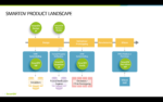
This is a key asset that has been developed and perfected by SmartDV over the years and provides a huge advantage to them. Refer to figure below. The SmartCompiler takes input in the form of a proprietary high-level language. The choice of design specification language, methodology, verification platform, etc., are specified in parameterized form. Standardized Linting rules built into the compiler ensure that variations in input style due to individual development engineer’s style are homogenized. The SmartCompiler technology eliminates the need to play with low-level specification and is able to quickly generate Design IP solutions and VIP solutions. These proprietary compilers, which are for internal use, have enabled SmartDV to get their IP solutions to the market, well ahead of others.

There are two different divisions within SmartDV, one for VIP and the other for Design IP. And there are two different compilers, one for generating VIP and another for generating Design IP. And these two compilers do not reuse or share any code.

SmartDV’s IP Solutions

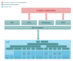
SmartDV currently offers 600 different Design and VIP solutions. That is an impressive array of IP solutions. Refer to the figure below for the extensiveness of their IP solutions covering the entire chip development lifecycle.

The SmartDV SmartCompiler technologies make their IP solutions easily scalable and rapidly customizable. As for portability, see below.

VIP Solutions

SmartDV’s verification solutions follow a modular architecture and consists of three layers. One is the hardware component that can run on an emulator or FPGA prototyping platform, one is software component that can run on a Linux machine and the third is the communication layer between these two. Because of this architecture and design, their VIP solutions are seamlessly portable.

Design IP Solutions

SmartDV’s IP are offered in high-level language form and thus are automatically portable.

The SmartDV Difference

Productivity/Turn-Around-Time

SmartDV is usually able to deliver new IP first to the market. They are able to develop a VIP solution from scratch with just 50% of the effort compared to others. And for developing subsequent platforms of the same IP, it takes just 25% of the effort compared to others. They are able to achieve these time/effort savings because of their modular architecture approach with VIP solutions. For example, they are able to generate an emulation model very quickly because the simulation model is reusable as the software layer within the emulation model.

Customization

Generally speaking, there is always some customization that is required of off-the-shelf IP. For this reason, most IP suppliers provide a user guide to provide insights to their customers on how to customize the IP. Usually, this customization process is not an easy one and could take lot of time away from the engineers.

With SmartDV, customers state the changes they want at a high level. This is mapped into the SmartDV’s proprietary high-level language for the SmartCompiler, which then generates the customized IP. Their compiler technology has matured to such a level over the last decade that multiple versions of any design can be easily generated by just tweaking the parameters that are input to the compilers. This makes it easy for customization to get the IP as exactly required. Click here for a press release that talks about a competitive benchmark example.

Customer Benefits

SmartDV Support

Technical support is provided by core development engineers rather than separate field applications engineers. Yes, Bipul’s title is director of applications engineering but the actual team he manages for providing customer support is made up of development engineers. And the support team is available 24×7. This is a huge benefit as it cuts down the time required to address the support needs.

Homogeneity Across Various IP Solutions

Because SmartDV’s IP solutions are generated by smart compilers, they all use the same architecture. Because of this homogeneity, once a customer has used one SmartDV IP, it is very easy to use other SmartDV IPs. As a result, customers can save lot of time on successive projects.

Complete Test Suites

SmartDV VIP solutions come with a complete test suite. Customers get the regression suite along with the scripts to run it. Not all IP houses provide this. And some charge for it. SmartDV includes this as a part of the IP products they deliver.

Summary

This interview with Bipul has provided lots of insights into how and why SmartDV has taken the market leadership position in the VIP space and why they are quickly gaining ground in the Design IP space. Understanding these aspects would come in handy when choosing one’s design and verification IP solutions for future chip projects. You can check SmartDV’s extensive IP solutions offerings at their Products Page. Their sweet spot IP solutions address MIPI, Video, Storage and Networking applications including RISC-V and ARM-based Networking SoCs.

Also Read:

SmartDV Shines in 2020!

SmartDV Expands Its Design IP Portfolio with an Acquisition

CEO Interview: Deepak Kumar Tala of SmartDV


ASML is the key to Intel’s Resurrection Just like ASML helped TSMC beat Intel

ASML is the key to Intel’s Resurrection Just like ASML helped TSMC beat Intel
by Robert Maire on 09-09-2021 at 6:00 am

TSMC INTEL ASML Hurricane 1

-Intel’s access to high-NA EUV tools may be their elixir of life
-TSMC’s EUV adoption helped it vault faltering Intel & Samsung
-Maybe ASML should invest in Intel like Intel invested in ASML
-Shoe is on the other foot- But cooperation helps chip industry

Intel is dependent upon ASML for its entire future
If Intel has any hope of recapturing the lead in the Moore’s Law race from TSMC then it desperately needs ASML’s help. Right now TSMC is miles ahead of Intel in EUV tool count and experience which is the key to advanced technology nodes. If both TSMC and Intel buy tools and technology at an equal rate, TSMC will stay ahead. The only other way for Intel to catch TSMC is for TSMC to fall on its own sword, much as Intel did, but we don’t see that happening any time soon.

Introduction of high-NA EUV is the next inflection point for Intel
Just as EUV was an inflection point that vaulted TSMC.

Back when ASML was struggling with EUV, making slow progress on a questionable technology, they were looking for an early adopter to take the plunge and convince the industry that EUV was real.

At the time, Samsung, TSMC and Intel were not signed up to EUV and viewed it very suspiciously. Nobody was willing to be the first to commit to it.

TSMC had famously said they would never do EUV
Then Apple changed all that by telling TSMC it needed to do EUV, for better chip performance, and Apple would write a check for it.

ASML got into a room with TSMC management and cut a deal and TSMC went from an EUV non-believer to a full on convert virtually over night. TSMC went from “never EUV” to its biggest customer and user (financed by Apple)
The rest is history.

TSMC’s earlier adoption of EUV helped it pull ahead of both Intel and Samsung over the past few years, aided by Intel’s production problems.

Its likely that TSMC may have pulled ahead without EUV but EUV really allowed TSMC to accelerate away from Intel and Samsung and create a huge Moore’s Law lead that exists today.

There is another similar inflection point coming up in the industry today, its high-NA EUV, basically the second generation of EUV technology. Similar to the first round of EUV there is hesitation in the industry as chip makers are unsure of the need for high-NA or its advantages or even whether it will arrive in time to make a difference.

ASML needs another early adopter to push the industry along.
Indeed, the IMEC roadmap, which most in the industry seem to be following does not call out the need for high-NA EUV.

Obviously there was some behind the scenes discussion between ASML & Intel as Intel came out with a full throated support of high-NA EUV technology.
If ASML anoints Intel as the high-NA EUV champion in exchange for its commitment and Intel gets preferential access to tools over TSMC as its reward, that could be the difference to get Intel back in the Moore’s Law game ahead of TSMC.

Not a slam dunk
There is of course a lot of risk but then again Intel has to take the risk as it has little choice. Will high-NA work? Will it be demonstrably better than current EUV? Will it get here in time? Will it be enough of an advantage over TSMC?

If the answer to enough of these questions is yes then Intel could win big, if not Intel could remain in a trailing position and never catch TSMC.

Intel of course has to do a lot of other things right, such as new transistor design and vertically stacked transistors but little of that will matter if they can’t get back in the Moore’s Law game with leading edge litho.

Maybe Intel should go from “Investor” to “Investee”
Back in 2012 ASML was struggling with EUV and needed some financial help to complete the technology and show support of customers. Customers were also pushing hard for 450MM wafer tools and demanding DUV tools, so ASML had its hands full, much like Intel today. It needed help in the form of money.

Intel, Samsung & TSMC each invested substantial sums in ASML. Intel invested and owned 15% of ASML, TSMC 5% and Samsung 3%.

All three companies made a killing in ASML stock as they sold after ASML’s stock ran up on EUV. Intel made enough to buy all the EUV tools it needed. Intel’s profits on its ASML investment helped prop up its weak performance.

It was a great deal for ASML and Intel, TSMC & Samsung, a true win/win which helped the industry adoption of EUV.

It would seem that now the shoe is on the other foot. ASML is on fire and Intel is in need of help. ASML has a 50% higher market cap than Intel.

Intel has a lot to do, a lot to prove and a lot of money to spend to recapture the lead in semiconductors. In short, Intel needs help.

Maybe ASML should invest in Intel much as Intel invested in ASML when the chips were down.

If ASML were to invest a similar amount in Intel, it would be enough cash to pay for both planned foundries in Arizona and then some. With enough left over for Intel to buy some expensive high-NA tools.

If it worked, as Intel’s investment in ASML did, ASML might make a killing in Intel’s stock as they regain their Mojo. Not to mention that ASML would get a great customer for high-NA.

This would certainly be better than a US government bailout of Intel’s self inflicted problems which would benefit investors rather than tapping taxpayers. Intel would certainly rather take the “free money” from the government.

Its a nice dream but we doubt that Samsung & TSMC would be happy with ASML investing in Intel.

The better, and somewhat logical solution, would be for Apple to write a check to Intel to be the sponsor for Intel’s high-NA EUV plans and Foundry projects in Arizona in return for first and guaranteed capacity to fab Apple’s chips at those fabs.

It would be great for Apple to have a second source that is US based rather than their total current reliance on TSMC in Taiwan (a short boat ride from the Chinese motherland). It would guarantee supply and keep pricing honest.

Apple certainly has the cash to support Intel as well as the need for another foundry source for leading edge as Samsung is clearly a “Frenemy” and not a great second source to TSMC.

Semiconductors remains very dynamic, global & highly interconnected
The linkage between chip makers and tool makers is much more than a customer supplier relationship. The semiconductor industry is a highly complex and dynamic industry of relationships that is ever changing with Intel going from the leader and “inventor” of Moore’s Law to struggling and ASML going from a distant third against Nikon and Canon to a monopolistic technology leader & powerhouse.

The fact is that relationships in the industry are the key to survival and success and navigating those relationships are key. The relationships are complex and multifaceted between chip makers & customers and tool makers but the reality is that no one can do it on their own and everyone is interdependent for the industry’s success…

The Stocks
We still maintain that Intel has a very long road in front of it with no assurance of success and many challenges. We maintain that Intel will be a “work in progress” for a relatively long time, well beyond most everyone’s investment horizon.

ASML is in an enviable position given its technology dominance and demand for its product. This positive environment will not change any time soon. ASML’s stock is priced for perfection but then again its in a perfect position so its hard to argue.

The semiconductor “shortage” is clearly longer lasting than expected as paranoia in the industry runs deep and everyone continues to double and triple order and stock up on inventory in an industry used to Kan Ban and just in time delivery.

The stocks have clearly slowed over the last few months as investors are rightfully wary of the end of the current “super duper cycle”. It remains difficult to put new money to work at current valuations.

Also Read:

KLA – Chip process control outgrowing fabrication tools as capacity needs grow

LAM – Surfing the Spending Tsunami in Semiconductors – Trailing Edge Terrific

ASML- A Semiconductor Market Leader-Strong Demand Across all Products/Markets


Can/Will NHTSA Rein in AVs Bad Boys?

Can/Will NHTSA Rein in AVs Bad Boys?
by Roger C. Lanctot on 09-08-2021 at 10:00 am

Autonomous Vehicle AV Bad Boys

There’s a new sheriff in town at the U.S. Department of Transportation in the form of Department Secretary Pete Buttigieg with an acting deputy in Acting Administrator Dr. Steve Cliff at the National Highway Traffic Safety Administration (NHTSA). NHTSA has served notice on bad boy Tesla CEO Elon Musk that it is investigating the circumstances connected with 11 fatal crashes of Tesla vehicles operating in Autopilot mode.

This is a key turning point in the industry for the undermanned and underfunded NHTSA. After four years without an administrator, the agency appears to be finally taking the reins, building a regulatory agenda (much of it already baked into the pending infrastructure bill), and slipping into the driver seat to guide the industry.

One of the higher profile and frankly embarrassing issues facing the agency has been periodic crashes of Tesla vehicles operating in Autopilot mode. Many of these crashes received high priority on-site investigative treatment by the agency and its regulatory cousin the National Transportation Safety Board (NTSB).

The NTSB most recently concluded that Tesla ought to be instructed to add an effective driver monitoring system and limit the use of Autopilot to divided highways. For its part, NHTSA expressed concern, but accepted Tesla’s dodges that A) drivers in fatal crashes of their vehicles were misusing Autopilot by not paying attention; and B) that data showed Tesla vehicles with Autopilot were safer to operate than non-Autopilot equipped vehicles.

The concern among regulators is clearly that other auto makers might follow Tesla’s lead, flooding highways with semi-autonomous driving systems being similarly misused resulting in similar fatal crash scenarios. It is perhaps for this reason that the agency sent a letter to George Hotz, founder of self-driving startup Comma.ai, expressing concern that the company’s aftermarket self-driving system would create hazardous driving circumstances for its users and other drivers sharing the road with them.

Hotz took two steps in response to the NHTSA outreach. He cancelled plans to introduce his aftermarket device, and he shifted to offering his software on a downloadable open source basis and sold the devices separately. Hotz also added a driver monitor to his device, which earned Comma.ai a top ranking in a Consumer Reports evaluation of self-driving systems.

Until now, both Musk and Hotz have found ways to work around NHTSA, while more traditional robotaxi developers, like Kyle Vogt at General Motors’ Cruise, have sought self-driving car exemptions from regulatory oversight by NHTSA. Safety advocates are outraged at the behavior of both NHTSA and Tesla. Tesla fans are thrilled with their cars and the freedom with which they are trusted to operate in semi-autonomous mode in their Tesla’s.

NHTSA certainly faces a challenge in coming to grips with the Tesla Autopilot application. It is clear that the system fails when it is being misused, but also fails when drivers are paying attention – there are multiple Youtube videos to attest to the wandering guidance of Tesla systems and their ability to mistake a Burger King sign for a Stop sign under the right circumstances.

There is an even more salient concern which is the challenge of properly activating and de-activating the system in the car. Regardless of the reliability of Tesla’s sensing systems, it is quite simple for a driver to make an incorrect selection in his or her attempt to turn on or maintain Autopilot – creating a significant gap between the driver’s expectations and the vehicle’s actual performance.

It remains to be seen whether NHTSA has the resources and expertise necessary to evaluate Tesla’s Autopilot – especially as the system itself is a moving target with regular updates of its algorithms and sensing capabilities. Perhaps NHTSA could start with the Tesla’s own warning message – most recently received by drivers of the Model 3 with Full Self Driving beta. The message stated: “(Your vehicle) may do the wrong thing at the worst time…(keep your) hands on the wheel and pay extra attention to the road.”

As soon as that message was sent to Tesla owners, NHTSA ought to have stepped in. It is comparable to GM telling owners of older model Chevrolet Bolts to park their cars outdoors. Of course, those Bolts were already subject to a NHTSA-initiated recall.

The latest initiative by NHTSA – to investigate Tesla crashes – is an effort to at least make an effort. Like President Biden said about climate change: Doing nothing is not an option. The best news of all is that NHTSA is no longer asleep at the wheel. It is an open question as to whether the Agency is ready to take the wheel. The bad boys of AV tech will be watching closely.


Verifications Horizons 2021, Now More Siemens

Verifications Horizons 2021, Now More Siemens
by Bernard Murphy on 09-08-2021 at 6:00 am

Aero DT min

In a discussion with Tom Fitzpatrick of Siemens EDA he recalled that their Verification Horizons newsletter started 17 years ago, back when they were Mentor. We’ve known about the Siemens acquisition for a while. The deal closed in March 2017, but it wasn’t until January 1, 2021 that the legal entity merger was complete. Which makes this the first version of the newsletter in which they’ve had enough time to absorb and express a Siemens slant to Verification Horizons.

Tom reiterated that a major motivation in the acquisition was filling out the Siemens vision of digital twins. These start from a big system view (like an aircraft for example). Mechanical, fluidics, thermal, software and so on. In modern systems there’s now so much new electronic content that modeling must also reach down inside those subsystems. The September issue of Verification Horizons covers multiple topics underlying this trend. I’ll just touch on a few.

Digital Threads, Twins, MBSE and IC Development

Model-based Systems Engineering (MBSE) is a new favorite topic of mine, driving modeling and design all the way from the ultimate system (e.g. an aircraft) down to SoCs. Siemens outlines a methodology called Arcadia which they use in their System Modeling Workbench to describe and decompose from high-level requirements and block functions down to individual components. SysML is a modeling language commonly used to describe behaviors and constraints at these higher levels.

How does IC design and particularly verification interact with these higher levels? In the example shown in the newsletter, they bridge using TLM (i.e. software) models for IC component behaviors, and verification of requirements through coverage analysis. In the aircraft example, they talk about a DO-254 list of requirements, each requiring a test and confirmation that the test passed. To this they would add coverage metrics to complete requirements coverage.

Verifying AI-enabled SoCs for HPC

Time to market pressures are just as active today in these SoCs as elsewhere, even though such systems are monsters and require very extensive hardware and software testing. (Much of what they describe in this article applies equally to big non-AI systems but I’m guessing this write up was motivated by an actual AI design experience 😀.) They talk here particularly about need for parallel development of hardware and software. This starts from a virtual platform and progresses to IP RTL development in parallel with driver development, and so on through to pre-silicon prove-out with apps and post-silicon bring-up.

The article makes the point that this style of development must be supported by a combination of emulation and prototyping. Emulation through hardware design development and early software apps development, since even here validation must comprehend hardware test loads. Prototyping during late hardware development and through software app development because there you need software performance. The article stresses the advantages of the Siemens two-part prototyping solution here: Veloce Primo for up to 12B gates and ICE support and Veloce ProFPGA for shipping prototypes to customers.

Verifying a DDR5 Memory Subsystem

I like talking about applications, so this is my last selection from the set of articles in the September newsletter. High bandwidth memory is more commonly integrated in big server processors, AI systems and other large SoCs. For this we we need even faster links from the main digital die(s) to these in-package DRAMs. The latest released standard here is DDR5, providing double the bandwidth at lower power than DDR4.

Siemens provides QVIPs for both chip and DIMM DDR5 memories. This write-up goes into quite a bit of detail on connecting and configuring your design. Plus creating compile and simulation scripts and running simulation and debug. I won’t attempt to summarize these other than to note they provide help in generating scenarios. Also assertions, transaction, performance analysis and more. If this is an area of interest to you, follow the link. They provide much more detail on all of these topics.

Lots of good material in this issue of Verifications Horizons. Tom also created his own blog post. Both well worth your time to read!

Also Read:

Optimize AI Chips with Embedded Analytics

AMS IC Designers need Full Tool Flows

Symmetry Requirements Becoming More Important and Challenging


Ansys IDEAS Digital Forum 2021 Offers an Expanded Scope on the Future of Electronic Design

Ansys IDEAS Digital Forum 2021 Offers an Expanded Scope on the Future of Electronic Design
by Daniel Nenni on 09-07-2021 at 10:00 am

IDEAS Banner ad

For those of you following the latest developments in electronic design it has become clear that the industry is transitioning through an inflection point that is shifting some of the ground rules of design. The increase in the speed and integration density in today’s systems are blurring the lines between chip design and system design, and is epitomized by multi-die, 3D integrated circuits. Multiphysics – the simultaneous analysis of multiple physical effects – is at the heart of another profound and challenging shift in electronic design practice. By merging previously distinct physics disciplines while adding novel physics into the equation, it is driving a step-function in the technical expertise required by electronic design teams.

Here Comes the Multiphysics Revolution

A concrete example of how the facts on the ground are rapidly evolving include the increasing focus on thermal analysis, as it has become apparent that heat dissipation is probably the #1 limiting factor in 3D-IC integration density. But thermal gradients across heterogeneous components inevitably leads to differential expansion, which results in mechanical stress and warpage of a package.

Warping impacts the system reliability directly, but temperature also has less direct design effects. For example, it determines the maximum current in wires to avoid electromigration reliability issues. The higher speeds of signals coupled with larger physical sizes of multi-die systems make electromagnetic simulation a must – for not just the radio frequency (RF) designers, but also for high-performance computing (HPC) and artificial intelligence/machine learning (AI/ML) hardware. Inter-related physical effects such as these are driving the multiphysics revolution.

New Signoff Requirements

The semiconductor foundries have responded to the rise in 3D-IC design starts by supplementing their sign-off requirements and their recommended IC design flows to include the thermal, electromagnetic, and other tools that were previously relegated to OSATs or other outside vendors following fabrication. Most of the advanced 3D systems that have been brought to market so far were designed by large, leading semiconductor companies that have the resources and expertise to take advantage of the new technical opportunities. But, in order to make 3D-IC design more accessible to mainstream design teams, the industry needs tools and design platforms that capture and automate these advanced multiphysics design requirements in practical workflows.

The old ways of working won’t cut it in this new reality. Design specialists with specific domain knowledge dispersed over multiple groups need to be brought together into vertically integrated design teams that make expertise available right from the get-go during system prototyping. Designers will need new tools, new training, and new methodologies to compete in this environment.

Register for IDEAS to Discover Leading Electronic Design Techniques

The best place to learn about the newest electronic design techniques from industry experts is to attend this year’s Ansys IDEAS Digital Forum: Innovative Designs Enabled by Ansys Solutions.

IDEAS is a digital event that takes place Sept. 22-23, 2021. It gathers many of the leading electronic design companies from across the world where you’ll access C-level executive keynote speeches as well as advanced techniques from leading-edge design teams. Take a look at the IDEAS Agenda to see the unparalleled breadth and scope of multiphysics tools, solutions, and practical implementations with 40 presentations in 10 technical tracks for electronic systems analysis, semiconductor signoff, photonics, cloud, and workflow solutions.

– Power Integrity – Silicon to System Reliability – 3D-IC & Electrothermal Analysis
– Voltage-Timing Signoff – Silicon Photonics – System Analysis & Simulation
– Low Power Design – Designing with Electromagnetics – Cloud & Workflow Automation

With a roundtable panel and executives from the design community and solution providers, you can get a quick and accurate impression of the state of the art in electronic design today – all from the comfort of your home office.

Registration for IDEAS is now open to all at ansys.com/ideas. Sign up and reserve your front seat for a showcase of the future of electronic design.

Also Read

Have STA and SPICE Run Out of Steam for Clock Analysis?

Extreme Optics Innovation with Ansys SPEOS, Powered by NVIDIA GPUs

Ansys Multiphysics Platform


IoT and 5G Convergence

IoT and 5G Convergence
by Ahmed Banafa on 09-05-2021 at 6:00 am

IoT and 5G Convergence

The Convergence of 5G and Internet of Things (IoT) is the next natural move for two advance technologies built to make users lives convenient, easier and more productive. But before talking about how they will unite we need to understand each of the two technologies.

Simply defined; 5G is the next-generation cellular network compared to 4G, the current standard, which offers speeds ranging from 7 Mbps to 17 Mbps for upload and 12 Mbps to 36 Mbps for download, 5G transmission speeds may be as high as 20 Gbps. Latency will also be close to 10% of 4G transmission, and the number of devices that can be connected scales up significantly which warranted the convergence with IoT. [1]

The Internet of Things (IoT) is an ecosystem of ever-increasing complexity; a universe of connected things providing key physical data and further processing of that data in the cloud to deliver business insights— presents a huge opportunity for many players in all businesses and industries. Many companies are organizing themselves to focus on IoT and the connectivity of their future products and services. IoT can be better understood by its four components: Sensors, Networks, Cloud/AI and Applications as showing in Fig.1.  [2,3,9]

Figure 1: Components of IoT

When you combine both technologies, 5G will hit all components of IoT directly or indirectly, sensors will have more bandwidth to report actions, network will deliver more information faster, for cloud and AI the case of real-time data will be reality, and applications will have more features and cover many options given the wide bandwidth provided by 5G.


Benefits of using 5G in IoT  

1. Higher transmissions speed

With transmission’s speed that can reach 15 to 20 Gbps, we can access data, files, programs on remote applications much faster. By increasing the usage of the cloud and making all devices depend less on the internal memory of the device, it won’t be necessary to install numerous processors on a device because computing can be done on the Cloud. Which will increase the longevity of sensors and open the door for more types of sensors with different types of data including high-definition images, and real-time motion to list few. [4]

2. More devices connected

5G impact on IoT is clearly the increased number of devices that can be connected to the network. All connected devices are able to communicate with each other in real-time and exchange information. For example, smart homes will have hundreds of devices connected in every possible way to make our life more convenient and enjoyable with smart appliances, energy, security and entertainment devices. In case of industrial plants, we are talking about thousands of connected devices for streamlining the manufacturing process and provide safety and security, add to that concept of building a smart city will be possible and manageable on a large scale. [4]

3. Lower latency

In simple words, latency is the time that passes between the order given to your smart device till the action occurs. Thanks to 5G this time will be ten times less than what it was in 4G. For example: Due to lower latency the use of sensors can be increased in industrial plants, including; control of machinery, control over logistics or remote transport all is now possible. Another example, lower latency led healthcare professionals to intervene in surgical operations from remote areas with the help of precision instrumentation that can be managed remotely. [4]

Challenges facing 5G and IoT convergence

  1. Operating across multiple spectrum bands

5G will not replace all the existing cellular technologies any soon, it’s going to be an option beside what we have now, and also new hardware needed to take full advantage of the power of 5G, IoT’s second component “networks” will have more options now and can deal with a wide spectrum of frequencies as needed, instead of being limited to few options. [5]

  1. A Gradual up-gradation from 4G to 5G

The plan is to replace 4G in a gradual way with all the infrastructure available now and this must be done on multiple levels and phases; software, hardware and access points. This needs big investment by both sides’ users and businesses, different parts of the nation will have different timelines to replace 4G and that will be created challenges in the services provided based on 5G, in addition the ability and desire of users to upgrade their devices to a “5G compatible “device is still a big unknown, a lot of incentives and education needed to convince individual and businesses to make the move. [5]

  1. Data interoperability

This is an issue on the side of IoT as the industry evolves, the need for a standard model to perform common IoT backend tasks, such as processing, storage, and firmware updates, is becoming more relevant. In that new sought model, we are likely to see different IoT solutions work with common backend services, which will guarantee levels of interoperability, portability, and manageability that are almost impossible to achieve with the current generation of IoT solutions. Creating that model will never be an easy task by any level of imagination, there are hurdles and challenges facing the standardization and implementation of IoT solutions and that model needs to overcome all of them, interoperability is one of the major challenges. [6]

  1. Establishing 5G business models

The bottom line is a big motivation for starting, investing in, and operating any business, without a sound and solid business models for 5G-IoT convergence we will have another bubble, this model must satisfy all the requirements for all kinds of e-commerce; vertical markets, horizontal markets, and consumer markets. But this category is always a victim of regulatory and legal scrutiny. [6]

Examples of Applications of 5G in IoT

1.    Automotive

One of the primary use cases of 5G is the concept of connected cars, enhanced vehicular communications services which include both direct communication (between vehicles, vehicle to pedestrian, and vehicle to infrastructure) and network-facilitated communication for autonomous driving. In addition to this, use cases supported will focus on vehicle convenience and safety, including intent sharing, path planning, coordinated driving, and real-time local updates. This bring us to the concept of Edge Computing which is a promising derivative of cloud computing, where edge computing allows computing, decision-making and action-taking to happen via IoT devices and only pushes relevant data to the cloud, these devices, called edge nodes, can be deployed anywhere with a network connection: on a factory floor, on top of a power pole, alongside a railway track, in a vehicle, or on an oil rig. Any device with computing, storage, and network connectivity can be an edge node. Examples include industrial controllers, switches, routers, embedded servers, and video surveillance cameras.”, 5G will make communications between edge devices and cloud a breeze [5,7]

2.    Industrial

The Industrial Internet of Things (IIoT) is a network of physical objects, systems, platforms and applications that contain embedded technology to communicate and share intelligence with each other, the external environment and with people. The adoption of the IIoT is being enabled by the improved availability and affordability of sensors, processors and other technologies that have helped facilitate capture of and access to real-time information.5G will not only offer a more reliable network but would also deliver an extremely secure network for industrial IoT by integrating security into the core network architecture. Industrial facilities will be among the major users of private 5G networks. [5,8]

3.    Healthcare

The requirement for real-time networks will be achieved using 5G, which will significantly transform the healthcare industry. Use cases include live transmission of high-definition surgery videos that can be remotely monitored. The concept of Telemedicine with real-time and bigger bandwidth will be reality, IoT’s sensors will be more sophisticated to give more in depth medical information of patients on the fly, for example a doctor can check up and diagnostic patients while they are on the emergency vehicle in the way to the hospital saving minutes that can be the difference between life and death. 2020’s pandemic taught us the significance of alternative channels of seeing our doctor beside in person, and many startups created apps for telemedicine services during that period, 5G will propel the use of such apps and make our doctor visits more efficient and less waiting [5]

 Ahmed Banafa, Author the Books:

Secure and Smart Internet of Things (IoT) Using Blockchain and AI

Blockchain Technology and Applications

Read more articles at: Prof. Banafa website

Article originally published in IEEE-IoT

 References

[1] https://davra.com/5g-internet-of-things/

[2] https://www.linkedin.com/pulse/iot-blockchain-challenges-risks-ahmed-banafa/

[3] https://www.linkedin.com/pulse/three-major-challenges-facing-iot-ahmed-banafa/

[4] https://appinventiv.com/blog/5g-and-iot-technology-use-cases/

[5] https://www.geospatialworld.net/blogs/how-5g-plays-important-role-in-internet-of-things/

[6] https://www.linkedin.com/pulse/iot-standardization-implementation-challenges-ahmed-banafa/

[7] https://www.linkedin.com/pulse/why-iot-needs-fog-computing-ahmed-banafa/

[8] https://www.linkedin.com/pulse/industrial-internet-things-iiot-challenges-benefits-ahmed-banafa/

[9] https://www.amazon.com/Secure-Smart-Internet-Things-IoT/dp/8770220301/


Podcast EP36: Semiconductor Design Acceleration

Podcast EP36: Semiconductor Design Acceleration
by Daniel Nenni on 09-03-2021 at 10:00 am

Dan and Mike are joined by Michael Johnson (MJ), CTO at NetApp. MJ provides “behind the scene” insights into NetApp technology and how it has quietly revolutionized information storage and management for chip design. The key enabling technologies along with specific use cases are discussed. MJ also discusses moving to the cloud and how NetApp addresses the major hurdles for this migration along with a specific customer example.

The views, thoughts, and opinions expressed in these podcasts belong solely to the speaker, and not to the speaker’s employer, organization, committee or any other group or individual.


The Arm China Debacle and TSMC

The Arm China Debacle and TSMC
by Daniel Nenni on 09-03-2021 at 6:00 am

Barnum and Baily Circus

Having spent 40 years in the semiconductor industry, many years working with Arm and even publishing the definitive history book “Mobile Unleashed: The Origin and Evolution of ARM Processors in Our Devices” plus having spent more than 20 years working with China based companies, I found the recent Arm China media circus quite entertaining.

While I have zero firsthand information on this situation I do have numerous contacts and have had discussions on the topic. I also have many years of experience with Arm management, enough to know that the Arm China situation as described in the media is complete nonsense.

Rather than rehash the whole fiasco, here are links to one of the inflammatory articles and a retraction, which is quite rare for today’s media. After publishing false information most sites just move on to the next topic leaving the fake news up in spite of the collateral damage. I would guess that Arm made some calls on this one, absolutely.

ARM China Seizes IP, Relaunches as an ‘Independent’ Company [Updated]

ARM Refutes Accusations of IP Theft by Its ARM China Subsidiary

This Arm China false narrative started as most do, with a misread publication and a provocative title with the sole purpose of feeding clicks to the advertising monster within. He didn’t even get the author of the original publication’s name right and that still has not been corrected:

“As Devin Patel reports...” It’s Dylan Patel, he is a SemiWiki member, and he said nothing about “ARM China Seizing IP”.  And by the way it’s Arm not ARM. That name was changed some time ago.

The author of the misfortunate article is a prime example of the problem at hand. While not the worst by any means, he has zero semiconductor education or experience. He does not know the technology, the companies, or the people, yet flocks of sheep come to his site for the latest semiconductor news. Pretty much the same as getting accurate political information from Facebook.

One of the reasons we started SemiWiki ten plus years ago was that semiconductors did not get their fair share of media attention. TSMC was a prime example. Even though they were the catalyst for the fabless semiconductor revolution that we all know and love, very few people knew their name or what they accomplished.

Now the pendulum has completely swung in the other direction with false TSMC narratives running amok. This one is my favorite thus far:

Intel locks down all remaining TSMC 3nm production capacity, boxing out AMD and Apple

And yes that one reverberated throughout the faux semiconductor media even though it was laughably false.

Here are a couple more recent ones that went hand-in-hand:

Taiwan’s TSMC asking suppliers to reduce prices by 15%

TSMC to hike chip prices ‘by as much as 20%’

Imagine the financial windfall here…

The upside I guess is that TSM stock is at record levels as it should be.  There is an old saying, “There is no such thing as bad publicity” (which was mostly associated with circus owner and self-promoter extraordinaire Phineas T. Barnum). The exception of course being your own obituary as noted by famed Irish writer Brendan Behan.

With today’s cancel culture, bad press can be your own obituary which is something to carefully consider before publishing anything, anywhere, at any time. Of course, there is that insatiable click monster that needs to be fed so maybe not.


Why Optimizing 3DIC Designs Calls for a New Approach

Why Optimizing 3DIC Designs Calls for a New Approach
by Synopsys on 09-02-2021 at 10:00 am

IC design engineering 3DIC 1024x615 1

The adoption of 3DIC architectures, while not new, is enjoying a surge in popularity as product developers look to their inherent advantages in performance, cost, and the ability to combine heterogeneous technologies and nodes into a single package. As designers struggle to find ways to scale with complexity and density limitations of traditional flat IC architectures, 3D integration offers an opportunity to continue functional diversity and performance improvements, while meeting form-factor constraints and cost.

3D structures offer a variety of specific benefits. For example, performance is often dominated by the time and power needed to access memory. With 3D integration, memory and logic can be integrated into a single 3D stack. This approach dramatically increases the width of memory busses through fine-pitch interconnects, while decreasing the propagation delay through the shorter interconnect line. Such connections can lead to memory access bandwidth of tens of Tbps for 3D designs, as compared with hundreds of Gbps bandwidth in leading 2D designs.

From a cost perspective, a large system with different parts has various sweet spots in terms of silicon implementation. Rather than having the entire chip at the most complex and/or expensive technology node, heterogeneous integration allows the use of the ‘right’ node for different parts of the system, e.g., advanced/expensive nodes for only the critical parts of the system and less expensive nodes for the less critical parts.

In this post, which was originally published on the “From Silicon to Software” blog, we’ll look at 3DIC’s ability to leverage designs from heterogenous nodes– and the opportunities and challenges of a single 3D design approach to achieve optimal power, performance, and area (PPA).

Adding a Vertical Dimension Changes the Design Strategy

While 3D architectures elevate workflow efficiency and efficacy, 3DIC design does introduce new challenges. Because of the distinct physical characteristics of 3D design and stacking, traditional tools and methodologies are not sufficient to solve these limitations and require a more integrated approach. In addition, there is a need to look at the system in a much more holistic way, compared to a typical flat 2D design. Simply thinking about stacking 2D chips on top of each other is insufficient in dealing with the issues related to true 3D design and packaging.

Since the designs must be considered in three dimensions, as opposed to the typical x, y aspects of a flat 2D design, everything must be managed with the addition of the z dimension  – from architectural design to logic verification and route connection – including bumps and through-silicon vias (TSVs), thermal, and power delivery network (PDN) opportunities for new tradeoffs (such as interposer based versus 3D stacks, memory on logic or logic on memory, and hybrid bonding versus bumps). Optimization of the ‘holy grail’ of PPA is still a critical guiding factor; however, with 3DICs, it now becomes cubic millimeter optimization, because it’s not just in two directions, but also the vertical dimension that must be considered in all tradeoff decisions.

Further complicating matters, higher levels of integration available with 3DICs obsolete traditional board and package manual-level techniques such as bump layout and custom layout for high-speed interconnects, which cause additional bottlenecks. Most importantly, interdependency of previously distinct disciplines now needs to be considered in a co-design methodology (both people and tools), across all stages of chip design, package, architecture, implementation, and system analysis.

Let’s look at an example of a specific design challenge – the goal to improve memory bandwidth. Traditionally, designers would look at how to connect the memory and CPU to get the highest possible bandwidth. But with 3DICs, they need to look at both the memory and CPU together to figure out the optimal placement in the physical hierarchy, as well as how they connect, through CSVs or silicon vias, for example. While performance is critical, designers need a way to evaluate the power and thermal impact by stacking these types of elements together in different ways, introducing new levels of complexities and design options.

Taking a Silicon-First Approach

While it might seem obvious to consider a 3D architecture in a similar manner as a printed circuit board (PCB) design, 3DICs should ideally take a silicon-first approach – that is, optimize the design IP (of the entire silicon) and co-design this silicon system with the package. Within our approach to 3DICs, Synopsys is bringing key concepts and innovations of IC design into the 3DIC space. This includes looking at aspects of 3DICs such as architectural design, bringing high levels of automation to manual tasks, scaling the solution to embrace the high levels of integration from advanced packaging, and integrating signoff analysis into the design flow.

3DICs integrate the package, traditionally managed by PCB-like tools, with the chip. PCB tools  are not wired to deal with both the scale complexity and process complexity. In a typical PCB there may be 10,000 connections. But in a complex 3DIC, there are hundreds of millions of connections, introducing a whole new level of scale which is far outpacing what older, PCB-centric approaches can manage. Existing PCB tools cannot offer assistance for stacking dies, and there is no package or PCB involved. Further, PCB tools cannot look at RTL or system design decisions. The reality is that there cannot be one single design tool for all aspects of a 3DIC (IC, interposer, package), yet there is an acute need for assembling and visualizing the complete stack.

The Synopsys 3DIC Compiler does just that. It is a platform that has been built for 3DIC system integration and optimization. The solution focuses on multi-chip systems, such as chip-on-silicon interposer (2.5D), chip-on-wafer, wafer-on-wafer, chip-on-chip, and 3D SoC.

The PPA Trifecta

Typically, when you think of large complex chips, the first optimization considered is area.  SoC designers want to integrate as much functionality into the chip and deliver as high performance as possible. But then there are always the required power and thermal envelopes, particularly critical in applications such as mobile and IoT (although also increasingly important in areas such as high-performance computing in a data center when overall energy consumption is prioritized as well). Implementing 3D structures enables designers to continue to add functionality to the product, without exceeding the area constraints and, at the same time, lowering silicon costs.

But a point tool approach only addresses sub-sections of the complex challenges in designing 3DICs. This creates large design feedback loops that don’t allow for convergence to an optimal solution for the best PPA per cubic mm2 in a timely manner. In a multi-die environment, the full system must be analyzed and optimized together. It isn’t enough to perform power and thermal analysis of the individual die in isolation. A more effective and efficient solution would be a unified platform that integrates system-level signal, power, and thermal analysis into a single, tightly coupled solution.

This is where 3DIC Compiler really shines–by enabling early analysis with a suite of integrated capabilities for power and thermal analysis. The solution reduces the number of iterations through its full set of automated features while providing power integrity, thermal, and noise-aware optimization. This helps designers to better understand the performance of the system and facilitate exploration around the system architecture.  And it also allows a more efficient way to understand how to stitch together various elements of the design and even connect design engineers in some ways to traditional 2D design techniques.

3DICs Are an Ideal Platform for Achieving Optimal PPA Per Cubic mm2

Through the vertical stacking of silicon wafers into a single packaged device, 3DICs are proving their potential as a means to deliver the performance, power, and footprint required to continue to scale Moore’s law.

Despite the new nuances of designing 3D architectures using an integrated design platform, the possibilities of achieving the highest performance at the lowest achievable power makes 3D architecture appealing. 3DICs are poised to become even more widespread as chip designers strive to achieve the optimum PPA per cubic mm2.

By Kenneth Larsen, Product Marketing Director, Synopsys Digital Design Group

Also Read:

Using Machine Learning to Improve EDA Tool Flow Results

How Hyperscalers Are Changing the Ethernet Landscape

On-the-Fly Code Checking Catches Bugs Earlier


Optimize AI Chips with Embedded Analytics

Optimize AI Chips with Embedded Analytics
by Kalar Rajendiran on 09-02-2021 at 6:00 am

Tessent Embedded Analytics Architecture

The foundry model, multi-source IP blocks, advanced packaging technologies, cloud computing, hyper-connectivity and access to open-source software have all contributed to the incredible electronics products of recent times. Along with this, the complexity of developing and taking a chip to market has also increased. And that is just from the effort perspective to implement a chip that performs to its specification. Add to this, the competitive market forces that demand faster time to market cycles.

While companies overcome these challenges by leveraging a combination of top-notch talent, tools, processes and proprietary methodologies, a new generation of chips are taking these challenges to a higher level. Artificial Intelligence (AI) driven applications such as security, visual cognition, and natural language comprehension/processing are behind the demand for these AI chips. Are time-proven techniques of overcoming time to market challenges sufficient when dealing with these AI chips? This is the backdrop for a whitepaper authored by Richard Oxland and Greg Arnot, both from Siemens EDA.

The whitepaper describes how new tools and methodologies may be required to help designers optimize hardware and software not only during the development phase but also after the chips are deployed in the field. It establishes that designers having intimate visibility into the operation of the chip is imperative for the on-time development of these AI chips. It explains how analytics capabilities embedded within these chips not only can help take a chip to market faster but also assist with optimizing the performance of the systems. This blog covers the salient points I gleaned from the whitepaper.

As embedded electronic systems get more complex, the interaction between hardware and software also becomes more complex. This makes debugging and optimizing for performance a very challenging and extremely time-consuming endeavor. Not only must root causes of bugs be determined and corrected but sub-optimal performance of a correctly functioning system must also be resolved under severe time-to-market pressures.

The authors discuss the Tessent Embedded Analytics platform and use an AI accelerator chip as an example to showcase the value product developers stand to gain from utilizing embedded analytics. The Tessent Embedded Analytics architecture has been designed and the platform implemented from the bottom up as a scalable, flexible and powerful solution to harness complexity in SoCs and embedded systems. The platform comprises a portfolio of silicon IP and software interface, together with APIs, an SDK, and database and IDE functionality. Refer to figure below.

Figure: Tessent Embedded Analytics Architecture

Source: Siemens EDA

The analytics platform combines IP and software designed to provide functional insights into complex SoC behavior. Tessent silicon IP can monitor internal bus transactions, processor execution, and other system-level activity within the device, correlated across the system, and at the right level of detail for the task in hand. The platform also contains the SW tools, APIs, and libraries required to process functional data and give designers a detailed understanding of the behavior of the hardware and software in the embedded system.

The whitepaper goes into details of how different embedded analytics modules bring value to the chip development process. Refer to figure below for the different analytics modules used with the AI accelerator chip. You can learn about all available embedded analytics modules by downloading the Tessent Embedded Analytics Product Guide.

Figure: Tessent Embedded Analytics Modules in an AI Accelerator Chip

Source: Siemens EDA

System Validation and Optimization

The customers for this example AI accelerator chip are Machine Learning (ML) application developers. Their software must be able to take advantage of all the unique hardware capabilities of the accelerator chip and maximize performance. As the limiting factor for system performance is the data throughput between memory and functional units, the chip design team must be able to optimize the high-bandwidth-memory (HBM) controller and memory banking schemes with confidence.

Assuming that memory corruption events are observed during the system validation phase, the team would have traditionally looked to simulation for debugging the issue. But as the use case is large, as in the case with many AI chips, debugging this way could consume many days or even weeks. This is where embedded analytics comes in as the savior. Using the supplied Python API and library of tests, the validation team configures the embedded analytics subsystem to find the root cause of the memory corruption. The DMA module is used to write to and examine the contents of the HBM in a precisely determined timeframe. The Bus Monitor is set up to look for transactions within a fixed address range and capture bus trace into a circular buffer. And the Enhanced Trace Encoder provides a mechanism to monitor the program execution of the relevant CPU.

With the memory corruption issue resolved, engineers can now focus on measuring response latencies of the HBM for different banking schemes using the built-in functionality of the Bus Monitor and the Python API. This mechanism allows for quick and easy experimentation with different hardware configurations.

Optimization in the Field

After system validation and optimization, a chip vendor may learn during field trials that the customers’ own applications may not be meeting expected performances. Fortunately, the same embedded analytics used during system validation can be leveraged to optimize memory bandwidth and latency.

Summary

The Tessent Embedded Analytics platform provides a solution that not only helps with the debug of an AI SoC during its development phase but also performance optimization of the product throughout its lifecycle. For full details, you can download the whitepaper here.

Also Read:

AMS IC Designers need Full Tool Flows

Symmetry Requirements Becoming More Important and Challenging

Debugging Embedded Software on Veloce