RVN! 26 Banner revised (800 x 100 px) (600 x 100 px)

Live 58th Design Automation Conference Coverage!

Live 58th Design Automation Conference Coverage!
by Daniel Nenni on 12-05-2021 at 10:00 am

Dan and Shushana Friday Harbor San Juan Islands

My beautiful first mate and I will be together at DAC this year. Her first DAC was 1985 in Las Vegas and we lived happily ever after. SemiWiki bloggers Tom Dillinger and Daniel Payne will also be at DAC attending sessions and meeting with exhibiting companies to learn and blog about the latest innovations inside the semiconductor ecosystem.

This year DAC will start with the traditional Sunday night reception and opening keynote: “EDA Growth Accelerates as Moore’s Law Slows” at 5pm on Sunday by Charles Shi, PhD, Vice President | Research Analyst, Semiconductors & Semiconductor Equipment, Needham & Company, LLC of Needham and Company. This is a must attend event for all EDA people.

Description:
It may be counter-intuitive to argue that electronic design automation (EDA) industry could see accelerated growth because Moore’s Law is slowing down. In this presentation, I will walk you through my reasons why such could be the case. We believe the slowing Moore’s Law has led to design diversification with domain-specific chip designs replacing one-size-fits-all designs, has motivated systems companies to enter the silicon race, and has nurtured the recent renaissance of semiconductor startups. EDA, IP, and foundry are key enablers and beneficiaries of these trends. In addition, the slowing Moore’s Law means chip-level scaling must be complemented with package- or system-level scaling, which creates a greater need for system design and analysis that will significantly expand the scope of EDA as well as its market size.

We are convinced that the strong growth of EDA in 2020 and 2021 was not a “Covid phenomenon” but the beginning of a new era that will feature strong double-digit growth for the EDA industry. Last but not least, we believe EDA can play a key role in mitigating the global chip shortage that may last beyond 2022, as foundries push more designs migrating to sub-20nm nodes. We argue design migration to sub-20nm nodes is an underappreciated alternative to ease chip shortage other than massive capacity additions at 28nm and above.

Charles joined our podcast last week if you would like to hear our banter on EDA. Next is the welcome reception. This is normally the best networking opportunity of DAC. If you are there please introduce yourself. It would be a pleasure to meet you all.

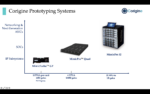
There will be a couple of interesting book signings on the exhibition floor. On Monday and Tuesday Wally Rhines will be signing free copies of his book “Predicting Semiconductor Business Trends” in the Infinisim booth #1652. My beautiful wife and I will be there as well. In booth #1543 S2C EDA will be giving away copies of my book “Prototypical II The Practice of FPGA Prototyping for SoC Design“. I will be there from 1-2pm on Monday and Tuesday for signings.

The rest of my time will be spent at the DAC keynotes and walking the exhibition floor meeting with friends and people who I consider family from the semiconductor ecosystem, absolutely

I hope to see you there!

About DAC

The Design Automation Conference (DAC) is recognized as the premier conference for design and automation of electronic systems.  DAC offers outstanding training, education, exhibits and superb networking opportunities for designers, researchers, tool developers and vendors.


A Next-Generation Prototyping System for ASIC and Pre-Silicon Software Development

A Next-Generation Prototyping System for ASIC and Pre-Silicon Software Development
by Kalar Rajendiran on 12-05-2021 at 6:00 am

Corigine Prototyping Systems

Every now and then, disruptive technology is brought to market, challenging the way things have been done to that point. We are all familiar with many such technologies. The rhetorical question is, how many of us were aware, recognized and acknowledged those technologies before they became well established? For example, a startup called Corigine has been rethinking prototyping and emulation solutions for semiconductor products. They are on a mission to make prototyping capability accessible to a wider audience of software and hardware engineers, right from their desktop. And to offer far greater onboard capability than is currently available on traditional prototyping solutions, thereby relieving some of the dependence on expensive emulation infrastructure. Corigine  expects to disrupt the widely used traditional prototyping/emulation model with their recently announced solutions. Before a product gets recognized and acknowledged for its value, awareness of the product needs to happen. This article is about bringing that awareness.

Before reviewing these products from Corigine, a little backdrop would be useful to understand the impact such solutions could bring to the prototyping and emulation market. Whether inventing or innovating, prototyping comes into play. During inventions, prototyping is part of the invention process. During innovations, though not essential, prototyping is invariably done for pragmatic reasons. The reasons include cost optimization and time to market reduction for the complete product. While the basic reasons for prototyping are to verify conformance to specifications and validate performance to customer/product expectations, there are other reasons too. Most products are not that useful without software running on them. Consequently, a product launch requires having both the hardware and software ready at that same time.  Software developers seek a head start rather than waiting for the hardware to be ready in its final form.

Hardware/software co-verification has become a very important aspect of product development, for integration of software (sw) with hardware (hw) well before final chips and boards become available. A good prototyping system should allow for not only ease of verification of the hardware but also enable hardware validation, software development, debugging and hw/sw integration. It is in this context that the two product announcements from Corigine are of interest. Corigine is a fabless semiconductor company that designs and delivers leading edge I/O and networking products, IPs and some EDA solutions.

In summer of this year, Corigine introduced a prototyping platform called the MimicPro™ system for SoC, ASIC and IP subsystem verification and pre-silicon software development. The platform makes prototyping capabilities easily accessible to hardware verification engineers and software developers at pre-silicon stage, thus shortening the R&D cycle for final products. It’s a system built using Xilinx UltraScale™ FPGAs with the goal of optimizing functionality and performance. The press release can be accessed here.

In November, Corigine expanded their toolkit in this space with their MimicTurbo GT card. This offering makes the capabilities accessible to engineers right at their desktop. Through a PCIe-based MimicTurbo GT card, Corigine makes silicon verification and software R&D right from an engineer’s desktop. The press release can be accessed here.

Requirements For Next-Generation Prototyping Solutions

A next-generation prototyping solution should cost-effectively enable hardware/software co-verification in addition to offering the following functionality.

  • Enable Software development
  • Greater automation, for partitioning and more
  • Necessary debug capabilities and system view
  • Multi-user access to hardware for cost-management
  • Useful scalability for handling small/simple designs to large/complex SoCs
  • Suitability for use over the cloud and within the enterprise
  • Security for IP in use

In addition, the automotive market has some very stringent safety requirements for semiconductor/electronic products that should be addressed by a prototyping solution.

Corigine Solutions

The following is a synthesis of what I gathered by reviewing/previewing Corigine’s product brochures on MimicPro and MimicTurbo GT solutions, respectively.

MimicPro FPGA Prototyping System

The system enables early software development, system validation and regression testing, while significantly reducing development time and workload. It offers a full system view with high visibility for rapid debug capability through a System Scope Logic Analyzer. Its automatic clock handling eliminates the need for manual handling of gating clock which is prone to errors and unnecessary engineering workload. The auto partitioning feature reduces the need for manual intervention by automating pin-muxing and instrumentation. While the system addresses all the requirements identified in the earlier section, the following are of special mention.

Scalability

  • Scales from 30 million gates to 1 billion gates (1 to 32 FPGAs)

Support for Automotive Safety

  • FMEDA, HIL, ADAS (ISO26262)
  • Fault injection-Force/Release capability that are essential for debugging and functional safety prototyping


MimicPro System


MimicTurbo GT Card

The Card can be deployed in a 16-lane PCI Express slot and supports 64 GTY transceivers (16 Quads) along with the essential I/O interfaces and includes FMC and FMC+ connectors. Bundled with the MimicTurbo software, the solution delivers the best-in-class automated partitioning for larger System-on-Chip designs. The MimicTurbo software leverages the Xilinx VU19P HSTPM IP for extraordinarily low latency with I/O pin-muxing across transceivers.

Deployment Ease

The Corigine MimicTurbo GT card is designed for quick installation in a PCIe system. The card is designed with the necessary interfaces and pre-built connectors that enables users to quickly deploy the hardware environment with the Xilinx® Virtex® UltraScale+™ FPGA XCVU19P. To further ease deployment, the card can be configured as a benchtop standalone platform as well.

Performance

The Corigine MimicTurbo GT offers automated FPGA partitioning and interconnect while leveraging the high-speed Xilinx GT (GigaHertz Transceiver) I/O connection between multiple FPGAs to deliver multi-gigabits per second performance.  The card provides GT pin muxing and automatic clock control, and features a sixteen-lane PCI Express interface along with DDR4 component memory for performance.

Scalability

The Corigine MimicTurbo GT provides modular upgradability from an entry point of a single FPGA card with 48 million gates to multiple cards deployed in a single or multiple PCIe systems.

MimicTurbo GT Card


Availability

MimicPro Systems: General availability of 1, 4 and 32-FPGA based systems. Configurations containing more FPGAs to follow.

MimicTurbo GT Card: Sample availability starts in December 2021.

Summary

The MimicPro system offers the scalability needed for verifying and validating completing SoCs and IP subsystems and delivers deep local debug capabilities for quicker elimination of bugs. The MimicTurbo GT card along with the MimicTurbo prototyping software solution simplifies the deployment of FPGA based prototyping at the desktop. Together, they greatly accelerate silicon verification and pre-silicon software development at semiconductor companies. The offerings are designed for deployment within the enterprise as well as over the cloud. These Corigine EDA solutions are architected to address the needs of SoCs for AI, Automotive, Communication, Processing and Vision applications.

You can access a copy of the MimicPro product brochure here. For a copy of the MimicTurbo GT product brochure, contact Corigine via marketing@corigine.com. For additional information, visit www.corigine.com.

Corigine @DAC 2021

You can meet with Corigine and check out their latest products at Booth 2443, Dec 6 -Dec 8, 2021.

DAC 2021 is being held at Moscone Center, San Francisco, CA

Also Read

Facebook or Meta: Change the Head Coach

The Roots Of Silicon Valley

CMOS Forever?


Podcast EP51: A Preview of the Needham Keynote at DAC

Podcast EP51: A Preview of the Needham Keynote at DAC
by Daniel Nenni on 12-03-2021 at 10:00 am

Dan is joined by Charles Shi, Vice President & Research Analyst for Semiconductors & Semiconductor Equipment at Needham & Company. Charles will be doing an opening keynote next week at the Design Automation Conference. He covers EDA as well as semiconductor equipment at Needham.

Dan explores why Charles is bullish on the EDA sector and what he sees ahead for the industry and its customers.

The views, thoughts, and opinions expressed in these podcasts belong solely to the speaker, and not to the speaker’s employer, organization, committee or any other group or individual.


CEO Interview: Da Chuang of Expedera

CEO Interview: Da Chuang of Expedera
by Daniel Nenni on 12-03-2021 at 6:00 am

Da Chuang CEO Expedera

Da is co-founder and CEO of Expedera. Previously, he was cofounder and COO of Memoir Systems, an optimized memory IP startup, leading to a successful acquisition by Cisco. At Cisco, he led the Datacenter Switch ASICs for Nexus 3/9K, MDS, CSPG products. Da brings more than 25 years of ASIC experience at Cisco, Nvidia, and Abrizio. He holds a BS EECS from UC Berkeley, MS/PhD EE from Stanford.

Tell us about Expedera?
Expedera has developed deep learning accelerator (DLA) IP that has the industry’s best performance per watt—18TOPS/watt. Our solutions are scalable to 128 TOPS with a single core and to PetaOps with multicore. We started from the ground up with a hardware/software codesign approach that enables us to deliver the most power efficient and scalable deep learning accelerator (DLA) for AI inference.

Our design outperforms other DLA blocks from leading vendors such as Arm, MediaTek, Nvidia, and Qualcomm by at least 4–5x. We’ve validated this using our 7nm test chip.

We are targeting AI inference, particularly for edge applications. We have at least one customer in this space currently in production—a top smartphone manufacturer.

My cofounders and I  founded Expedera in 2018. Our office is in Santa Clara.

What problems/challenges are you solving?
We provide a highly efficient AI inference solution. If a customer needs deterministic performance or a guaranteed level of performance with the best possible power and area efficiency, we can do that. If they need a solution that doesn’t require off-chip memory, we can do that. If they need a flexible, future-proof solution that can handle mixed models, we can do that. We also bring efficiency to model deployment because our co-designed platform reduces software complexity dramatically and ensures predictable performance.

What markets does Expedera address today?
We have announced a top-10 smartphone customer, so it’s fair to say mobile and edge AI are a sweet spot for us. Because of our scalability and determinism, we are a good fit for automotive and industrial automation. In fact, we are engaged with customers from GOPS to PetaOPS.

What are the products Expedera has to offer?
Our Origin deep learning accelerator IP platform addresses a wide variety of AI inference applications. The platform includes silicon IP and a comprehensive SDK built on TVM  that provides a Compiler that achieves out-of-the-box high performance.  The platform allows us to easily support different precisions and features—it’s very flexible.

What keeps your customers [architects, system designers] up at night? 
The reality is that most AI processors are underperforming and stall at around 30-50% utilization or less —wasting most of their potential TOPS. So system architects and designers overdesign their SoC to address unpredictable performance. Expedera provides predictable, deterministic performance with 90% utilization. Greater utilization results in better throughput for customers. Our platform gives architects the end-to-end visibility needed to right-size their AI-accelerator solutions early in the development cycle.

Another issue is the difficulty, the delays, and the uncertainty in model deployment. Data scientist can spend tremendous amounts of time to achieve minimal performance improvement.  With Expedera, engineers can deploy trained models without further changes. That increases confidence in the design, and avoids difficult development tradeoffs, bottlenecks and product uncertainty.

What added value do you bring to your customers?
Confidence in their solution. Efficient operation. Ease of deployment. Reduced BOM costs.

Providing an AI-solution as an IP has huge implications for both our business and our customers. The IP licensing approach allows us to address a broad set of edge-AI markets, and potentially license to leading vendors that already hold large shares in these markets. At the same time, we can enable startups and new market entrants that may not have the in-house expertise to design their own AI hardware and would otherwise be unable to participate or compete with incumbents.

What makes Expedera unique?
We’ve taken a fundamentally different approach to AI acceleration, in part, because we come from a networking background. We’ve taken a network-centric approach—rather than the CPU-centric approach—to neural network processing. We are able to segment the neural network into packets which are essentially command streams that can be efficiently scheduled and executed by our hardware in a very fast, efficient and deterministic manner. Additionally, our co-design approach enables a simpler software stack and a more productive and system-aware design and development experience.

What’s driving the company’s global expansion/growth?
The market expectation of AI-everywhere is driving growth and creating a competitive necessity for ODMs to provide increasingly intelligent and autonomous products. We are still in the hockey stick of AI deployment.

Also Read:

CEO Interview: Pradeep Vajram of AlphaICs

CEO Interview: Charbel Rizk of Oculi

CEO Update: Tuomas Hollman, Minima Processor CEO


Low Power High Performance PCIe SerDes IP for Samsung Silicon

Low Power High Performance PCIe SerDes IP for Samsung Silicon
by Tom Simon on 12-02-2021 at 10:00 am

SerDes IP for PCIe

No matter how impressive the specifications are for an SoC, the power performance and area of the finished design all depend on the IP selected for the IO blocks. In particular, most SOCs designed for consumer and enterprise applications rely heavily on PCI Express. Because PCIe analog IP is critical to design success, Samsung has developed a solid relationship with the IP provider Analog Bits that was highlighted in a talk given by Analog Bits Executive VP Mahesh Tirupattur at the recent Samsung Advanced Foundry Ecosystem (SAFE) Forum. The talk is titled “PCIe/CXL SERDES- Gen4/5 Enterprise Class Serdes & Lowest Power Gen3/4 Consumer SERDES in Samsung 28nm to 5nm Processes”. Mahesh offers extensive information on their SERDES IP on Samsung processes from 32nm in 2012 up the present with their 7LPP and 5LPE support in 2021.

SerDes IP for PCIe

According to Mahesh, their primary focus is in helping their customers to create highly differentiated designs targeted at customer needs. To this end they focus on low power, small silicon footprint and flexible configurations, among other things.

For the consumer market, Analog Bits delivers PCIe Gen2 and Gen3 with multiprotocol ability for SATA, eDP, XFI, etc. Their full rate architecture offers industry leading picojoules per bit combined with the lowest system and BOM cost. They support wire bond packages (up to 10G) and integration with clock chips. Their small form factor lowers silicon costs. Lastly, they include some programmability to the supported protocols.

Their enterprise and high performance PCIe SERDES offer Gen4/5 and extensibility to support SAS4, Ethernet, etc. Designs can have lane counts of 195 to over 300 placed on all multiple sides. They offer automotive grades and provide multiple channel and chassis support with channel equalization. These SERDES have been used in data center storage, GPUs, aggregators, bridges, re-timers and AI/ML.

Analog Bits’ PCIe SERDES can be arrayed to varying link widths, i.e. x1, x2, x4, x8, x16. Lanes can be independently programmed to support any PCIe spec, SAS, Ethernet, etc. They also offer flexibility for placement anywhere on an SOC and wider packaging options to improve cost and performance. One of his slides highlights the low power obtained for PCIe Gen3 in 28 FDSOI and 28LP Bulk. Coming in at 0.1 sq mm they both have similar PCIe power and dynamic power, ~54mW and ~6.8 mW/Gbps respectively. The FDSOI leakage of 30.5 microWatts betters the LP Bulk at 46.6 microWatts.

Mahesh spends some time discussing sample layouts for low power SERDES in wire bond packages. He includes test result eye diagrams at 5Gb/s, 8Gb/s and 10Gb/s that all look wide open and clear. Even the eye diagram for the high-performance full rate PCIe Gen4 SERDES that is used on Samsung NVMe SSD is impressive. It uses 117.7 mW per lane at 16Gbps (7.35mW/Gbps) in an area of 0.26 sq. mm.

Analog Bits has silicon proven test chips and also production tape outs for their Gen3 and Gen4 SERDES on Samsung 7LPP/5LPE. The Gen4 silicon is 1-16G with power coming in at 6 pj/bit. The Gen 3 is 1-8G with power at 4pj/bit. Gen5/SAS4 is on Samsung 8LPP with working silicon. Its stats are 0.583 sq. mm and 7.6 pj/bit, and is configurable across multiple lanes.

The presentation goes into extensive detail on test results and available layout configurations. I highly recommend the presentation because of the level of detail that it provides. Analog bits has a long term history developing IP for the full range of Samsung processes. As noted above it is impressive that Samsung chose Analog Bits to provide SERDES IP for their own NMVe. The presentation is available at analogbits.com/analog-bits-pcie-cxl-serdes-in-samsung-video/

Also Read:

On-Chip Sensors Discussed at TSMC OIP

Package Pin-less PLLs Benefit Overall Chip PPA

Analog Sensing Now Essential for Boosting SOC Performance


Continuous Integration of RISC-V Testbenches

Continuous Integration of RISC-V Testbenches
by Daniel Nenni on 12-02-2021 at 6:00 am

RISC V Results

In my last blog post about AMIQ EDA, I talked with CEO and co-founder Cristian Amitroaie about their support for continuous integration (CI). We discussed in some detail how their Design and Verification Tools (DVT) Eclipse Integrated Development Environment (IDE) and Verissimo SystemVerilog Linter are used in CI flows. Cristian gave a fascinating example: AMIQ EDA runs CI lint checks every few hours on the contents of the Github repository for the Universal Verification Methodology (UVM) reference implementation, and makes the results publicly available. Any time that anyone contributing to this project checks in new or changed code, it will be linted quickly. This helps to improve the quality of the code, and publishing the reports fits the whole open-source ethos.

Cristian concluded by hinting that this same process could be applied to other SystemVerilog/UVM design and verification IP available from public repositories. Last week we found out what he meant, in a new press release announcing that they have set up a CI flow for the open-source UVM RISC-V verification environment from OpenHW Group. The members of the group are using the AMIQ EDA tool results to enhance the quality, portability, and readability of their code. I asked Cristian to tell me more and, when we talked, he was kind enough to bring along Mike Thompson, the OpenHW Group Director of Engineering, Verification Task Group and Gabriel Raducan, R&D Team Lead at AMIQ EDA. Here are the highlights of our conversation.

Thanks for joining me today. Can you please start by telling me about OpenHW Group?

Mike: I expect that your readers know about RISC-V, the widely adopted free and open instruction set architecture (ISA). Many companies, organizations, and academic institutions have developed processor cores, verification tools, and many kinds of supporting software for this ISA. Of course, there is widely varying quality across these offerings. We formed OpenHW Group to develop very robust and flexible RISC-V open-source cores and best-in-class open-source verification testbench environments.

Cristian: We’re seeing increasing interest in RISC-V among our users. It’s clearly a hot topic in the industry.

So where does AMIQ EDA come into the picture?

Mike:  As individual members of the OpenHW Group use their own simulators to develop testbenches, it is important to have readable and maintainable SystemVerilog/UVM code that can run on any commercial simulator. We looked for a lint tool that could play the central role in this effort, but there are few, if any, open-source or commercial linters that support testbench code, particularly SystemVerilog/UVM. I looked at the available options and tried Verissimo because I heard good things about it.

Cristian: Mike contacted us, and we collaborated to set up an environment to check the OpenHW testbench code with our tool and then deploy it.

What does that mean? What specifically did you do?

Gabriel: There were really four parts to the project. The first was us doing some initial linting runs on the testbench and discussing the results with Mike and members of his team.

Mike: Next, Gabriel explained that the rules to be checked by Verissimo are highly customizable and he proposed an initial set. We worked together to refine this set to fit our verification goals. If we didn’t deem a particular rule important, it was easy to waive or suppress the check.

Gabriel: The third phase was setting up the CI flow that we mentioned in the press release. Any time that anyone in the Verification Task Group checks in code, it is linted within a few hours and the results are posted openly in a dashboard format. These regression runs ensure that everyone’s contributions meet the OpenHW coding guidelines and quality metrics. Finally, we added the rule and waiver files to the OpenHW repository so that they are accessible to the team.

Isn’t this a whole lot like the UVM CI flow we talked about last time?

Cristian: It’s really very similar; in both cases we run regular lint regressions on an open-source repository. Engineers working on open-source projects invest a lot of time and energy, and we are happy if we can help. We see this as an ongoing collaborative process from which both parties benefit. In fact, we constantly monitor OpenHW discussions on Github to help with linting topics and interact with more team members.

Have you found any issues with the RISC-V testbench code in this process?

Mike: Yes, we have fixed many dozens of issues reported by Verissimo. Some were violations of our SystemVerilog/UVM coding guidelines that we previously had no automated way to detect, and some were due to rules we had not considered before. I especially like the rules that warn us about constructs that may work inconsistently on different simulators or that are not even supported on all simulators. It is important for our code to be vendor-neutral and portable.

Could you give some examples of these issues?

Gabriel: Sure! SystemVerilog prohibits using a null class in a logical expression. Some simulators allow this, but we report it as non-standard code. UVM specifies that the Verilog “$random” call should be avoided, but we found a few usages in some older testbench code. We also detected some cases of overrides that didn’t actually make any changes to the base classes, which is a waste of simulation time and resources.

How has the experience been working together?

Mike: AMIQ EDA has been a wonderful partner. They’ve been proactive, responsive, and fully supportive of our project goals.

Cristian: The same is true of Mike and the OpenHW folks. Like our other advanced users, their feedback is extremely valuable in improving our products and adding useful new features.

Where do you go from here?

Mike: I think that Verissimo is now an indispensable part of our RISC-V testbench development efforts. We are using GitHub issues to track lint violations flagged by Verissimo so that individual members can address the issues found in their sections of code. This will be an on-going process. Even with only a few months of experience so far, I can’t imagine not having Verissimo in our flow.

Thank you both very much for your time.

Cristian and Gabriel: Thank you, Dan, and thank you, Mike, for making time to join us today.

Mike: Thanks to the three of you as well; it’s been a pleasure!

Also Read

Continuous Integration of UVM Testbenches

What’s New with UVM and UVM Checking?

Why Would Anyone Perform Non-Standard Language Checks?


Ansys to Present Multiphysics Cloud Enablement with Microsoft Azure at DAC

Ansys to Present Multiphysics Cloud Enablement with Microsoft Azure at DAC
by Daniel Nenni on 12-01-2021 at 2:00 pm

Picture1 1

Ansys and Microsoft  collaborated extensively over the past year to optimize and test Ansys’ signoff multiphysics simulation tools on the Azure cloud. Microsoft has invited Ansys to present the joint results in Azure’s DAC booth theater in San Francisco this year.

Two presentations are planned: covering the enablement of Ansys RedHawk-SC™ for power integrity signoff, and discussing electromagnetic simulation of large electronic systems with Ansys HFSS™.  Today’s advanced node designs and compact 3D-IC systems can require large amounts of compute resources to verify, which makes them ideal candidates for distributed processing in the cloud.

Microsoft Azure and Ansys have set up and tested both tools on Azure to determine the optimal hardware and system configurations for maximum speed, usability, licensing, and resource efficiency. These performance results will be revealed using real customer examples by examining the impacts of memory size and instance counts on throughput.

The Ansys-Azure collaboration results will be presented live at the Microsoft Azure DAC booth #1253 on:

  • Monday 6th at 3:15PM – Ansys HFSS on Azure
  • Tuesday 7th at 12:15PM – Ansys RedHawk-SC on Azure

These are key data points for any electronic designers moving to the cloud or interested in hearing about the state-of-the-art in cloud computing. If you can’t make it to DAC this year, see these blogs for more information: “Ansys RedHawk-SC on Azure: Hold on to Your Socks” and “How Azure FX VM Makes Ansys RedHawk-SC™ Run Faster the Less You Spend”.

About Ansys
If you’ve ever seen a rocket launch, flown on an airplane, driven a car, used a computer, touched a mobile device, crossed a bridge or put on wearable technology, chances are you’ve used a product where Ansys software played a critical role in its creation. Ansys is the global leader in engineering simulation. Through our strategy of Pervasive Engineering Simulation, we help the world’s most innovative companies deliver radically better products to their customers. By offering the best and broadest portfolio of engineering simulation software, we help them solve the most complex design challenges and create products limited only by imagination. Founded in 1970, Ansys is headquartered south of Pittsburgh, Pennsylvania, U.S.A. Visit www.ansys.com for more information.

Also Read

Big Data Helps Boost PDN Sign Off Coverage

Bonds, Wire-bonds: No Time to Mesh Mesh It All with Phi Plus

Optical I/O Solutions for Next-Generation Computing Systems


Webinar: The Backstory of PCIe 6.0 for HPC, From IP to Interconnect

Webinar: The Backstory of PCIe 6.0 for HPC, From IP to Interconnect
by Mike Gianfagna on 12-01-2021 at 8:00 am

The Backstory of PCIe 6.0 for HPC From IP to Interconnect

PCIe, or peripheral component interconnect express, is a very popular high-speed serial computer expansion bus standard. The width and speed the standard supports essentially defines the throughput for high-performance computing (HPC) applications.  The newest version, PCIe 6.0 promises to double the bandwidth that the current PCIe 5.0 specification offers. The standard is still a bit away from full release and mainstream deployment, but it is a highly anticipated technology that promises to set new benchmarks for performance throughout the industry. Samtec and Synopsys have teamed up to present a very interesting webinar on the topic. Read on to learn the backstory of PCIe 6.0 for HPC, from IP to interconnect.

Any high-speed communication channel requires two primary ingredients, IP to process the signals and a physical medium to deliver those signals. In a past life, my company developed high-speed SerDes (serializer/deserializer) IP. We are quite proud of its capabilities to deliver robust signals at high speed over long distances. Those were just academic projections until we teamed up with Samtec. They developed a high-precision copper cable that was several meters long. That medium really allowed to prove our point and we turned heads at many trade shows with the demo we created with Samtec.

The Demo

Similarly, an early PCIe 6.0 implementation requires IP to process the signals, a physical signal path and a set of stimuli to show what can be achieved. In this context, Synopsys provides the PCIe 6.0 IP and Samtec provides the physical connectivity and signal activity. A rather impressive demo has been developed to showcase what can be achieved with this emerging standard. The demo has been shown live recently at DesignCon, AI Hardware Summit, and most recently at Supercomputing (SC21). Note Samtec has a history of interesting demos at DesignCon. A video of this demo will be shown during the webinar. While quite interesting, this is not the main benefit of attending the webinar. More on that in a moment. First, a summary of the demo.

Thanks to its new DesignWare IP for PCIe 6.0, the Synopsys PHY generates four 64 GT/s PAM4 differential signals (PCIe 6.0  data rate). The differential pairs route through an Isola Tachyon® 100 G test board, to a Samtec 70 GHz Bulls Eye® High-Performance Test System cable assembly, the BE-70A Series.   The signal travels from the Bulls Eye connector, through 8” of low-loss coax cable, to precision 1.85 mm Samtec compression mount jacks, mounted on the first HSEC6 SI Evaluation Board.

The signals then travel about 30 mm in the board to the HSEC6 connector, and then to the second evaluation board. The differential pair exits the second evaluation board through another set of 1.85 mm compression mount jacks, through another 8” of coax cables, and are received back to the Bulls Eye test cable system, on the Synopsys board. The data routes back to and is recovered by the Synopsys PCIe receiver.

The results of the demo are eye-popping. During the webinar, you will learn all about bit error rates and see the eye diagrams. While impressive, there is a lot more to learn by attending this webinar.

The Backstory

This demonstration vehicle is one of the first interoperability platforms for PCIe 6.0 in the industry. There is much to be learned here, including practical signal channel design techniques and connectivity options. These are nuggets that are hard to get in a trade show environment. You need 1:1 access to experts who have the time to discuss the details. This is what you will get in this webinar.

The webinar is presented by two technology experts. Matthew Burns presents for Samtec. Over the course of 20+ years, he has been a leader in design, technical sales and marketing in the telecommunications, medical and electronic components industries. Mr. Burns holds a B.S. in Electrical Engineering from Penn State University.

Madhumita Sanyal presents for Synopsys. She has over 16 years of experience in design and application of ASIC WLAN products, logic libraries, embedded memories, and mixed-signal IP. Madhumita holds a Master of Science degree in Electrical Engineering from San Jose State University and LEAD from Stanford Graduate School of Business.

The webinar will be held on Wednesday, December 8, 2021, from 10:00 AM – 11:00 AM Pacific Standard Time.  You can register here. If PCIe 6.0 is in your future this is a great opportunity to get a head start. Seeing a demo at a trade show is useful but getting the details of what is happening behind the scenes and what design considerations are important can be invaluable.  Now you know the backstory of PCIe 6.0. 


Creative Applications of Formal at Intel

Creative Applications of Formal at Intel
by Bernard Murphy on 12-01-2021 at 6:00 am

formal image min

One of the sessions I enjoyed at the Synopsys Verification Day 2021 was a presentation on applying formal to a couple of non-traditional problem domains. I like talks of this kind because formal can sometimes be boxed into a limited set of applications, under-exploiting the potential of the technology. Intel have built a centralized team of formal experts who seem to be quite aggressive in exploring new ways to leverage their expertise and tools. The first of these talks was on using formal to root-cause problems found post-silicon and the second was on validating datapath implementations.

Applying formal property verification to post-silicon

Anshul Jain gave this talk and opened by acknowledging that there is skepticism about applying formal to post-silicon debug; he agrees this isn’t easy. He does a nice job of walking through challenges and explains a recipe Intel have developed over many years to help them apply formal most effectively in the context of these challenges. I won’t attempt to explain the details other than to note a few. Formal can handle blocks, not full chip, so they brainstorm their way with designers to likely block candidates. They use cover properties to work their way towards pre-conditions for failure. They aim to constrain judiciously, with simulation state in areas that are not critical to the failure, with under-constraints around the sensitive area. All good basic engineering judgment.

Eventually they converge on a root cause. Importantly, they use this reactive analysis to enhance proactive property checks for next generation designs. He cited one example in which they were able to find 8 post-silicon bugs over the last year. Which they spun into new pre-silicon checks, finding 6 bugs in the next generation design. Pretty good ROI!

Datapath formal verification

Datapath functions are notoriously resistant to formal methods, however Synopsys seems to have solved that problem with their datapath validation (DPV) technology. This is based on equivalence checking with a reference rather than property checking. Disha Puri talked about Intel’s ground experiences in what works best for their needs.

The default use model is to compare an RTL implementation against a C/C++ reference. This works but suffers from complexities in software optimizations in the reference for virtual modeling needs or other reasons unrelated to ultimate implementation. Then there are mapping choices – between what interfaces do you want to check equivalence? Also optimizations in the synthesis step. Getting to closure on a check can take significant effort, which may need to be repeated on minor changes in the source. Still a worthwhile task for an initial pass and signoff, but burdensome for iterative development.

Instead they tried RTL to RTL equivalence checks, using a legacy RTL as a reference. Still using DPV. I’m guessing conventional EQ would be hopeless on datapaths. They used this flow on Media designs and a graphics unit, building regression suites in one generation which they applied to the next generation and found 90+ bugs in a matter of weeks.

Equivalence checking without an obvious reference

Disha talked also about methods to apply DPV when they don’t have a reference model. For example, in extended math functions, they don’t have effective C++ references. A need of this kind arises for example when a big  new block is added to a datapath element. Apparently, it is possible to trigger bounded model checking in DPV. The use this feature to apply a simple property check. She said this had a simple setup, quickly checked a lot of opcodes and found 15 bugs. Property checking can still have value in datapath verification!

Very nice couple of talks. You can learn more from the recorded session. This session is listed about 2/3 of the way through Day 1.

Also Read:

Synopsys Expands into Silicon Lifecycle Management

CDC for MBIST: Who Knew?

AI and ML for Sanity Regressions


CEO Interview: Mo Faisal of Movellus

CEO Interview: Mo Faisal of Movellus
by Daniel Nenni on 12-01-2021 at 6:00 am

Mo Faisal Movellus

Prior to founding Movellus, Dr. Faisal held positions at semiconductor companies such as Intel and PMC Sierra. Faisal received his B.S. from the University of Waterloo, and his M.S. and Ph.D. from the University of Michigan, and holds several patents. Dr. Faisal was named a “Top 20 Entrepreneur” by the University of Michigan Zell Lurie Institute.

Tell us about Movellus?
Movellus is a leading supplier of Intelligent Clock Network IPs for high performance SoCs in AI, datacenter and Mil-Aero markets.

When we were helping companies develop high performance clocking structures we realized there was an opportunity to innovate in this area especially when it comes to clock distribution.

We worked closely with a number of innovative AI companies to create the next generation clock distribution networks that are intelligent, aware and self correcting.  This work culminated in Maestro, an Intelligent Clock Network IP Platform.

Maestro is a new architectural approach that has added smarts to the clock networks but also has opened up opportunities for architects to re-think the data flow on a chip. The result is we can put an “idea clock” anywhere on an SOC.

What problems/challenges are you solving and the evolution of the company over the years? 
There are two main problems we’re solving in high performance SoCs. First we’re increasing the area of synchronization in an SoC. For example you build a large 20mmx20mm array of compute elements that are fully synchronous. It improves the performance in inference AI chips significantly.

In addition to greater architectural flexibility, ICN benefits timing closure, making the process more predictable and consistent. Another significant benefit is the reduction in power without any loss in performance, this is achieved by recovering OCV, skew, jitter losses in the distribution network.

Now let me tell you about the power savings. Power has become extremely important in data center SoCs as it directly affects the total cost of ownership. Reducing a data center SoC’s power by 30% directly results in millions of dollars saved in energy cost.

What markets does Movellus address today? 
We have a range of customers, but mostly clustered around AI and related applications.  Esperanto is an example of a datacenter AI customer, we worked with them early on. They were very quick to understand the benefits and make great use of the core technology.

Two other markets that leverage our strengths are, Mil Aero because of our Rad Hard support and Automotive because of the test coverage/observability.  These two markets we stumbled upon when they came to us and asked if they could use Rad Hard libraries as the target for our TrueDigital technology.

The cool thing is to see our customers realize significant performance benefits architectural innovations using Maestro. This year we got to announce Mythic, Achronix and Syntiant, all leaders in their respective markets and fantastic partners.

What makes Movellus unique?
When we solve problems or invent technology for our customers, we always take a holistic approach. It has been part of our DNA since the inception of the company to consider the system, methodology, testability, flexibility, scalability of every solution we deliver. We’re in the business of creating high impact architectural innovation or enabling our customers to do it.

Our team consists of a special kind of “crazy” engineers. I like to say that the Movellus team might be the only team in the world where you can find an engineer that has deep experience in analog, digital, architecture, methodology and software design all in the same person. For example, you’re not going to find an engineer in the industry that can do phase noise analysis on an 8GHz oscillator while also being an expert at physical design, STA and even DFT.

This breadth in our team allows us to solve system level problems for our customers as opposed to just optimizing a small little IP block in isolation. This is an extremely valuable characteristic of our team that has resulted in us becoming architecture partners with our customers.

Now let’s not forget about the uniqueness of our technology. Our core technology is TrueDigital synthesizable nonlinear functions such as frequency generation and multiplication. Instead of inventing new ways of “synthesizing” nonlinear functions, we created new all-digital architectures that are implementable as digital logic using RTL to GDS design flows. That has opened us to a world of opportunities to solve problems that our customers face at the SoC level. We are the only company that can ship softIP for these applications, giving our partners and customers unprecedented flexibility.

What’s next for Movellus?
At this point, we have only just scratched the surface of what is possible. We can see a future where Maestro can help mitigate issues such as supply droop and simultaneous switching, the Ldi/dt problems as they’re known in the high performance chip world.

Another big opportunity is in the chiplet market where we can really help clock delivery, but that is a topic for another day… It is an amazing time for us and it’s no longer about wires and buffers, it’s about the intelligence in the whole system now. Throughput, Workload Management, Fmax, TOPS/watts and many more aspects are heavily influenced by the Clock Distribution Networks.

Also read:

Advantages of Large-Scale Synchronous Clocking Domains in AI Chip Designs

It’s Now Time for Smart Clock Networks

Performance, Power and Area (PPA) Benefits Through Intelligent Clock Networks