Sondrel is the trusted partner of choice for handling every stage of an IC’s creation. Its award-winning define and design ASIC consulting capability is fully complemented by its turnkey services to transform designs into tested, volume-packaged silicon chips. This single point of contact for the entire supply chain process ensures low risk and faster times to market. Headquartered in the UK, Sondrel supports customers around the world via its offices in China, India, Morocco and North America.
Introduction
Early in the SoC development cycle, Product Managers, Systems Architects and relevant technical stakeholders discuss and elaborate product requirements. Each group tends to have a specific mental model of the product, typically with product managers focusing on the end-use and product applications. At the same time, Systems Architects focus on functionality and execution and implementation of the requirements.
The ‘Requirements Capture Phase’ identifies, formulates and records all known functionality and metrics, including performance in a clear and complete proposal. In addition, this exercise identifies functionality that is not fully understood or may be included later and seeks to determine and plan what tasks are required to complete the qualification and quantification of such functions.
On completion, or as complete as possible at the program’s start, the system architecture team’s requirements go through an analysis phase with appropriate inputs from design and implementation teams. The outcome of this iterative process is an architecture design specification that includes an architecture design for which all functionality, estimation of the power, performance and area are determined.
The inclusion of design and implementation effort at the initial phase ensures better accuracy and validation for the specification and architecture. In addition, it identifies the sensitivities needed to guide design choices.
The architecture analysis includes the architecture exploration, IP selection/specification, verification of requirements, and generation of the project execution plan with major tasks to be elaborated in later phases.
The architecture exploration of the candidate architecture is a significant component. It refines the architecture design by modelling the proposal and evaluating known or reference use cases, dynamically allowing the system topology to be defined and provisioning of resources to be allocated (memory, bus fabric data/control paths etc.).
While it allows aspects of the functionality to be evaluated and validated (connectivity, timing, performance etc.) for confidence in the correctness of the design, later phases using more detailed and accurate models are used to determine and correct potential errors during the implementation of the architecture.
The remaining sections of this article cover the use of modelling in the architecture phase of the program.
SoC application use case capture for system architecture exploration
The initial part of SoC Architecture Exploration is a rigorous way of capturing one or more application use cases and dataflows which an SoC is required to perform. Accurate and complete description of use cases is necessary to communicate with stakeholders and agree on requirements early in the product definition phase.
The Systems Architect seeks to draw out the product requirements and express them so that technical and non-technical stakeholders can keep up with the product intent and architectural choices without excessive technical detail.
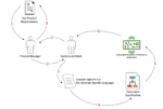
Figure 1 shows an overview of this collaboration process in 8 steps:
- Market analysis, industry trends, product requirements definition carried out by the Product Manager for a potential SoC solution
- Product Usecase requirements are communicated to the System Architect, usually by presentations, spreadsheets or documents.
- Requirements translation to DSL format required by modelling flows
- Tools generate an Executable Specification and visualisations of the use case
- Tools also generate the cycle-accurate SystemC model required for use case architecture exploration
- Systems architect inspects results of an exploration exercise and progressively converges to an optimal architecture for the SoC
- System Architect communicates findings with Product Manager
- The Product Manager may decide to modify requirements or collaborate with the Systems Architect to further refine the candidate SoC Architecture.
Industry trends show that vision-based applications are becoming more common to incorporate classical computer vision techniques and neural-net-based AI inferencing, with a fusion step to combine results from the two stages.
Figure 2 shows a typical autonomous vision use case data flow graph, with nodes representing processing functions and edges representing data flow. The specific stages are:
- Frame Exposure – The interval during which a camera sensor takes a snapshot of its field of vision. The image sensor may be configured in either global shutter or rolling shutter mode, and each mode has an exposure period associated with it.
- Frame RX – The interval over which pixes of an image grouped in lines are sent to the SoC over a real-time interface such as MIPI CSI-3.
- Image Conditioning – Any image pre-processing, filtering or summarisation steps performed on the received data before the actual compute stages.
- Classical Computer Vision – Well-known vision processing algorithms, for example, camera calibration, motion estimation or homography operations for stereo vision.
- Computational Imaging – Vision algorithms are augmented with custom processing steps such as Pixel Cloud or Depth Map estimation
- AI Inferencing – Neural Net based image processing for semantic segmentation, object classification and the like.
- Data Fusion – Final stage sensor fusion and tracking. May also include formatting or packetisation processing.
- Data TX – Can be over PCIE or a real-time interface such as MIPI CSI-3 at a constant or variable data rate.
Associated with every processing stage are parameters that need to be specified so that the dynamic simulation model can be configured correctly. These parameters generally describe:
- Read DMA characteristics: Number of blocks, block sizes, memory addresses and memory access patterns
- Processing characteristics: The delay which the task will require in order to perform its processing.
- Write DMA characteristics: Number of blocks, block sizes, memory addresses and memory access patterns
Figure 3 shows that this information is best described in tabular format, where rows represent processing tasks and columns are parameters associated with the task.
The use case graph may also have an embedded sub-graph, which is often the case with AI applications that describe the algorithm in terms of a Neural Network computation graph. Figure 4 shows a sub-graph within a larger use case graph. The method of describing the sub-graph is in the same tabular format, which may be present in any part of the larger graph, not just with AI processing.
Usecase parameters captured in tabular format as shown in Figure 3 are sufficient to describe the application intent regarding dataflows between processing stages and the processing delay of a given stage. The added benefit of having the graph drawn to the left of the table is that it becomes intuitive to understand the data flow, hence the relationship between nodes as processing stages. Even for large graphs, the method is applicable and offers supplementary information readily available if required.
Separate to the Application Usecase is a model of the Hardware Platform, which will perform the data transfers and processing delays as prescribed by the Usecase model. The Hardware Platform model will typically have the following capabilities:
- Generate and initiate protocol compliant transactions to local memory, global memory or any IO device
- Simulate arbitration delays in all levels of a hierarchical interconnect
- Simulate memory access delays in a memory controller model as per the chosen JEDEC memory standard.
Figure 4 shows a block diagram of one such Hardware Platform, which, in addition to a simulation model, forms the basis for elaborating an SoC architecture specification.
So far we have defined two simulation constructs – the Application Usecase Model and the Hardware Platform Model. What is required is now a specification of how the Usecase maps on to the Hardware Platform subsystems. That is, which tasks of the application usecase model are run by which subsystems in the hardware platform model. Figure 6 shows a the full simulation model with usecase tasks mapped on to subsystems of the hardware platform.
The Full System Model in Figure 6 is the dynamic performance model used for Usecase and Hardware Platform Exploration.
Every node in the Usecase graph is traversed during simulation, with the Subsystem master transactor generating and initiating memory transactions to one or more slave transactors. As a result, delays due to contention, pipeline stages or outstanding transactions are applied to every transaction, which cumulatively sums up the total duration that the task is active.
The temporal simulation view in Figure 7 shows the duration active for each task for a single traversal of the Application Usecase. The duration for the entire chain is defined as the Usecase Latency. Having one visualisation showing the Hardware Platform, Application Usecase and Temporal Simulation view often work very well for various stakeholders because it is intuitive to follow.
Now a single traversal is not useful, decides providing some sanity checks about the setup of the environment. For thorough System Performance Exploration multiple traversals need to be run, and in this setup, we see the two phases of the simulation. A transient phase is when the pipeline is filling up, followed by the steady-state when the pipeline is full; hence the system is at maximum contention.
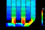
Figure 8 highlights a portion of the simulation when the system is at maximum contention. During the steady-state, metrics are gathered to understand the performance characteristics and bounds of the system. This guides further tuning and exploration of the use case and hardware platform.
Figure 9 shows two configurations of the hardware platform and the resulting temporal views. One system is setup for low latency by using direct streaming interfaces to avoid data exchange in the DDR memory.
Yet again, the benefits of showing the two systems visually bring clarity so that all stakeholders can understand with a bit of guidance.
The complete architecture exploration methodology relates to use case and platform requirements, simulation metrics, key performance indicators and reports.
Figure 10 shows the flow of information in the following order:
- Application Usecase is defined first. The tabular format for capturing the use case is crucial here, as shown previously in Figure 3
- Usecase Requirements associated with the Application Usecase are stated.
- Usecase Requirements are converted into Key Performance Indicators, which are thresholds on metrics expected from simulation runs.
- Simulation metrics are collected from simulation runs
- Usecase performance summary report is produced by checking if metrics meet their Key Performance Indicators or not.
A similar flow applies to Hardware Platform Requirements whereby:
- Hardware Platform defined first
- Platform Requirements stated
- Platform KPIs extracted from Requirements
- Platform simulation metrics collected
- Platform performance summary generated by comparing metrics with KPIs.
Also read:
Sondrel explains the 10 steps to model and design a complex SoC
Build a Sophisticated Edge Processing ASIC FAST and EASY with Sondrel
Sondrel Creates a Unique Modelling Flow to Ensure Your ASIC Hits the Target