As the oldest and largest EDA conference, the Design Automation Conference (DAC) brings the best minds together to present, discuss, showcase and debate the latest and greatest advances in EDA. It accomplishes this in the form of technical papers, talks, company booths, product pavilions and panel discussions.
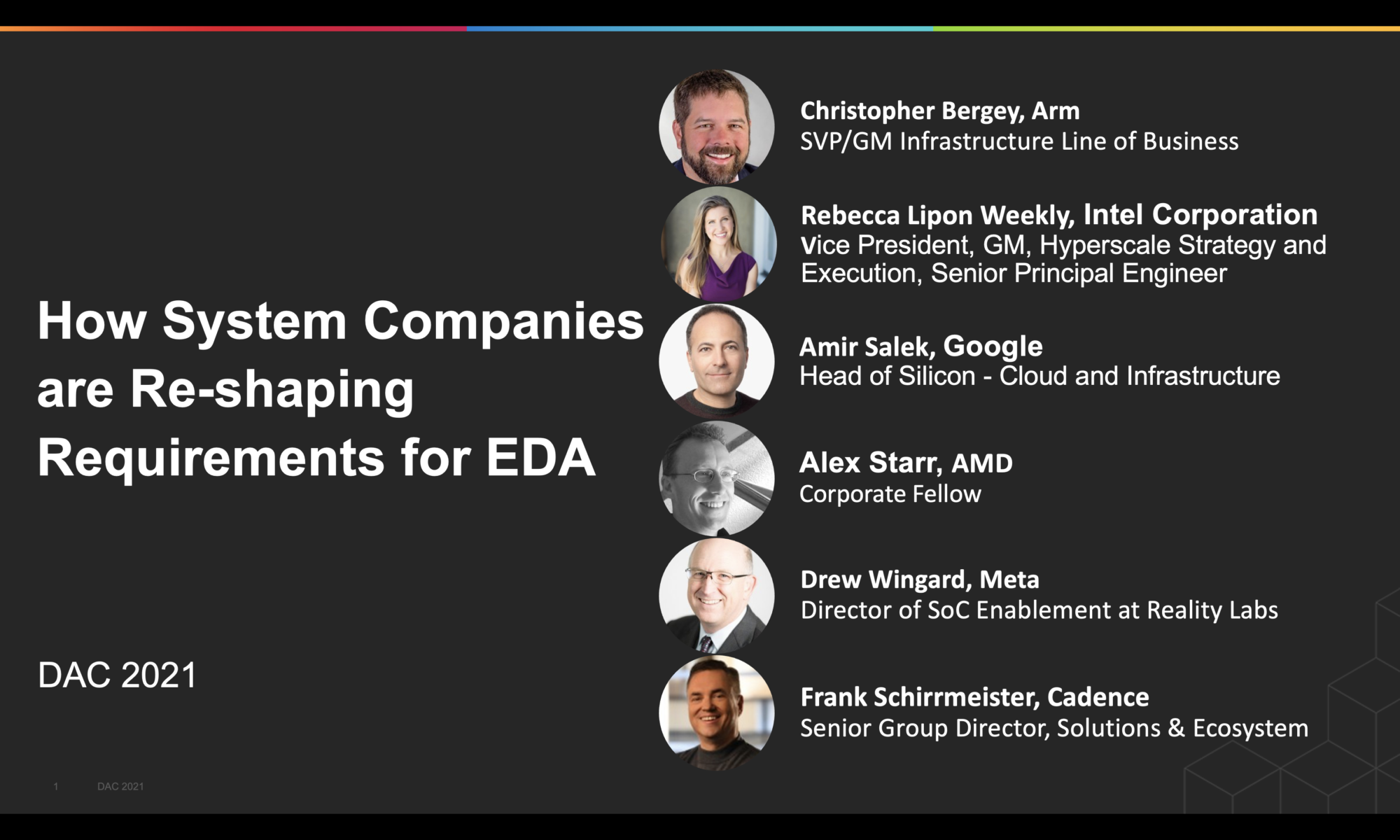
A key aspect of driving advances in design automation is to discuss evolving EDA requirements, so the industry can develop the solutions as the market demands. At DAC 2021, Cadence sponsored an interesting panel session that gets to the heart of this. The session was titled “How System Companies are Re-shaping the Requirements for EDA,” with participants representing Arm, Intel, Google, AMD and Meta (Facebook). The discussion was organized and moderated by Frank Schirrmeister from Cadence Design Systems.

The following is a synthesis of the panel session on EDA requirements to support the upcoming era of electronics.
Frank Sets the Stage
Referencing a Wired magazine article, Frank highlights how data center workloads increased six-fold from 2010 to 2018. Internet traffic increased ten-fold and storage capacity rose 25x over that same time period. Yet data center power usage increased only 6% over the same period and we have semiconductor technology, design architectures and EDA to thank for it.
The electronics industry is entering an era of domain-specific architectures and languages, as predicted by John Hennessy and David Patterson back in 2018, The primary factors driving this move are hyperscale computing, high-performance edge processing and the proliferation of consumer devices. The next generation of hyperconnected, always-on consumer devices are expected to deliver user experiences never imaginable even a few years ago.

The Global DataSphere quantifies and analyzes the amount of data created, captured and replicated in any given year across the world. End point data creation growth is estimated at a CAGR of 85% from 2019 to 2025 and 175 Zettabytes in 2025. It is as much as there are grains of sand on all the world’s beaches. That’s quite a bit of data to be processed and dealt with.
The companies on the panel session are all involved in creating, analyzing, capturing and/or replicating this humongous amount of data. The discussion will cover what they see as their requirements on the EDA industry.
Arm – Chris Bergey
From an infrastructure perspective, Arm’s involvement is from HPC to data center to 5G to edge gateways. Specialty computing is a big focus area now. System validation is key, when customers are committing to large R&D expenses. When dealing with chiplets architectures leveraging 2D/2.5D/3D implementations, it is relatively easier when all the dies and design rules are owned by a single company.
For heterogeneous implementations, multi-chip packaging is generally used in markets where the margins are high enough to accommodate the extra design efforts, yield fallouts and margin stacking. In reality, hybrid chiplets implementations will help the market grow faster. The EDA industry is expected to play a big role in making heterogeneous chiplets implementation easier and robust.
Intel – Rebecca Lipon
High Bandwidth Memory (HBM) and high-speed servers drove development of critical IP that opened the floodgates for a whole bunch of new applications and products. The industry has to maintain its determination to continue on similar journeys and try to push the envelope. For example, IP level innovation at the packaging level.
Open Compute Project (OCP) is the foundation started by Meta a decade ago. Many companies including all of the companies represented on the panel today are members of this foundation. It works on initiatives that allow you to use open firmware and software that speeds up development and extends the life of products.
One of the initiatives that OCP is focused on is composable computing and supporting domain specific architectures. EDA industry should look into this and look to Linux as a model for open-source community.
Google – Amir Salek
The number of categories of workflows that run in our global data centers, is in the 1000s. And Google Cloud adds a whole new dimension to the demand on serving and processing data, supporting different workloads. Each workload has its own characteristics and while many of them can run on general-purpose hardware, many more need customized hardware.
Testing and reliability are primary areas of concern. I think this plays a major role in terms of understanding the causes of marginality and to decide how to deal with. Looking at TPU pods, we’re talking 1,000s and 1,000s of chips that are stitched together to work in coordination as a supercomputer. So, any little bit of a reliability issue during testing and test escapes, basically gets magnified. And then after many days, you find out that the whole effort was basically useless and you have to repeat the job again.
Prototyping FPGA is a tremendous platform for testing and validation. We are doubling down on emulation and prototyping every year to make sure that we close the gap between the hardware and software.
AMD – Alex Starr
The data center all the way to the consumer, the whole software stack needs to run on whatever the solution is. And many of our designs are implemented using chiplets architecture and that brings up different types of complexity to deal with. The things that keeps me up at night is how to verify and validate these complex systems and get to market quickly.
Hardware emulators and FPGA prototyping systems market is booming and is probably the highest growth area within EDA. Today’s emulators can fit very large designs and help prototype bigger devices. The hardware acceleration platforms to put large designs are tremendously expensive and difficult to get working at that scale. And, as designs grow to five plus billion dates, emulators are not going to scale. Emulation as used for prototyping is at its limit. We are looking at hybrid kind of modeling-based approaches. We are refining these internally and in collaboration with external standards bodies. We really want to extend out into our OEM customers and their ecosystems as well.
Meta (Facebook) – Drew Wingard
We are working on chips to enable our vision for the Metaverse. Metaverse involves socially acceptable all-day wearables such as augmented reality glasses. This new computing platform puts an enormous amount of processing resources right on one’s face. The result is that it demands very tight form factors, low power usage and very minimal heat dissipation.
We need to put different parts of processing in software and hardware. We need to think a lot about the tradeoffs between latencies vs throughputs and cost of computation vs cost of communication. We need a mix of options around different classes of heterogeneous processing and a whole lot of support around modeling. And we have to balance the desire for optimizing requirements versus offering optionality because nobody knows what the killer app is going to be.
As a consumer firm, privacy is incredibly important as they relate to our product usage. Our products should be socially acceptable for the persons wearing as well as the persons across from them.
When we roll all the above together, availability of system models and design cycle times become incredibly important. Many challenges revolve around availability of models and interoperability between models. This is where continuing to closely work with the EDA industry opens up opportunities.
Also Read
2021 Retrospective. Innovation in Verification
Methodology for Aging-Aware Static Timing Analysis
Scalable Concolic Testing. Innovation in Verification
Share this post via:


Comments
There are no comments yet.
You must register or log in to view/post comments.