At the ISS conference held from April 4th through 6th I presented on who I thought would have the leading logic technology in 2025. The following is a write up of that presentation.
ISS was a virtual conference in 2021 and I presented on who currently had logic leadership and declared TSMC the clear leader. Following that conference, I did a lot of calls for investment firms, and I was often asked when Intel would catch TSMC, my answer was unless TSMC stumbled, never.
A year later the foundries are stumbling, and Intel is accelerated, can Intel catch up?
I reviewed some Intel history, discussed their leadership throughout the 2000s and then how in the 2010s they began to fall behind, I discussed why I thought this happened.
I have previously published on Intel’s issues here.
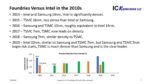
The bottom line is 2014 through 2019 Samsung and TSMC each introduced 4 nodes while Intel introduced 2, the Intel nodes were bigger individual density jumps but when you chain together the 4 foundry jumps, they increased density more than Intel and took the lead. Figure 1. summarizes this.
Figure 1. Foundries Versus Intel in the 2010s.
Figure 1 only illustrates the “nodes” from Intel, they weren’t standing still, for 14nm they released 5 versions all with the same density but with progressively improving performance and for 10nm they released 4 versions, once again with the same density but improving performance (note the last version has now been renamed 7nm).
By 2020 Samsung and TSMC both had 5nm in production and compared to Intel 10nm they are denser processes. TSMC had taken a lager jump from 7nm to 5nm then Samsung and was the clear leader with the densest process, smallest SRAM cell size and the industries first silicon germanium FinFET. Figure 2. summarizes this.
Figure 2. 2020 Comparison.
In 2021 the foundries have slowed down.
Samsung 3nm has encountered yield issues and we believe in 2022 their 3GAE (early) process will be used almost exclusively for internal products with 3GAP (performance) being released to external customers in 2023. Samsung chose to go to Horizontal Nanosheets (HNS) for 3nm (a type of gate all around process Samsung calls Multibridge). I believe HNS production issues are still being worked out and Samsung’s interest in being first to HNS has led to delays and poor yields.
TSMC did risk starts of their FinFET based 3nm process in 2021 but production is now pushed to late 2022 with products in the industry in 2023. In 2019 TSMC had risk starts of 5nm and by late 2020 iPhones were shipping with TSMC 5nm parts, for 3nm we won’t see iPhones until 2023. TSMC has also reduced the density for this process from an original 1.7x target to ~1.6X with reduced performance targets.
While Samsung and TSMC were experiencing delays, Intel announced, “Intel Accelerated”, an aggressive roadmap of 4 nodes in 4 years. This is truly accelerated when you consider 14nm took 3 years and 10nm took 5 years. I was frankly skeptical of this when it was announced but at the recent investors event Intel is pulling in the most advanced 18A process from 2025 to 2024!
Our view from now to 2025 is as follows:
2022 – Intel 4nm process, Intel’s first EUV use with a 20% performance improvement over 7nm. Intel had formerly talked about a 2X density improvement for this generation but is now just saying a “significant density improvement”, we are estimating 1.8X. Samsung 3nm will likely be for internal use only with a 1.35X density improvement, 35% better performance at the same power and 50% lower power at the same performance. The density improvement is not very impressive but the performance and power improvements are, likely due to adoption HNS. TSMC 3nm is FinFET based and will provide an ~1.6X density improvement with 10% better performance at the same power and 25% lower power at the same performance.
2023 – Intel 3nm process with 18% better performance, denser libraries and more EUV use. We estimate a 1.09X density improvement making this more of a half node. Samsung 3GAP should be available to external customers and TSMC 3nm parts should appear in iPhones.
2024 – in the first half Intel 20A (20 angstrom = 2nm) process is due with a 15% performance improvement. This will be Intel’s first HNS (they call it RibbonFET) and they will also introduce back side power delivery (they call this PowerVia). The backside power delivery addresses IR power drops while making front side interconnect easier. We are estimating a 1.6X density improvement. In the second half of 2024 Intel’s 18A process is due with a 10% performance improvement. We are estimating a 1.06X density improvement making this another half node. This process has been pulled in from 2025 and Intel says they have delivered test devices to customers.
2025 – Samsung 2nm is due in late 2025, we expect it to be a HNS and because it will be Samsung’s third generation HNS (counting 3GAE as the 1st generation and GAP as the 2nd generation) and their previous generations have been relatively less dense we are forecasting a 1.9X density jump. TSMC has not announced their 2nm process yet other than to say they expect to have the best process in 2025. We may see 2nm in 2024 but for now we have it placed in 2025, we expect a HNS process and are estimating a 1.33X density improvement. We believe the density improvement will be modest because it is TSMC’s first HNS and because the 3nm process is so dense that further improvements will be more difficult.
Figure 3 illustrates how Intel may “flip the script” on the foundries by doing 4 nodes while the foundries do 2.
Figure 3. Density jumps.
We can now look at how Intel, Samsung, and TSMC will compare in density out to 2025. We also added IBM’s 2nm research device based on their 2nm announcement. Figure 4. presents both density versus year and node.
Figure 4. Transistor Density Trends.
From figure 4 we expect TSMC to maintain the density lead through 2025.
The most complex part of our analysis is illustrated in figure 5 where we compare performance. It is very difficult to compare processes to each other for performance without having the same design run on different processes and this rarely happens. The way we generated this plot is as follows:
- The Apple A9 process was run in both Samsung 14nm and TSMC 16nm and Tom’s hardware found the same performance for both versions, we have normalized performance at this node to 1 for both Samsung and TSMC.
- From the 14/16nm node through 3nm we have used the companies announced performance improvements to plot relative performance. For 2nm we have used our own projections.
- We don’t have any designs that ran on Intel processes and either Samsung or TSMC. However, AMD and Intel both make X86 microprocessors and AMD microprocessors on TSMC 7nm process have competed with Intel 10nm Superfin processors with similar performance and we have set Intel 10SF to the same performance as TSMC 7nm. This is not ideal and assumes that both companies have done an equally good job on design but is the best available comparison. We have then scaled all the other Intel nodes from the 10SF based on Intel’s announcements.
- Once again, we have place IBM’s 2nm on this chart based on their 2nm announcement.
Figure 5. Relative Performance Trends.
Our analysis leads us to believe Intel may take the performance lead both on a year basis and a node basis. This is consistent with Intel’s stated goal of taking the “performance per watt lead”. Assuming TSMC is referring to density their statement that they will have the best process in 2025 could also be true.
In conclusion we believe Intel has been able to significantly accelerate their process development at a time when the foundries are struggling. Although we don’t expect Intel to regain the density lead over the time period studied, we do believe they could retake the performance lead. We should get another good read on progress by the end of 2022 when we see whether Intel 4nm comes out on time.
Also Read:
The EUV Divide and Intel Foundry Services