Charles Shi, semiconductor analyst at Needham & Company, an US-based investment bank and asset management firm, hosted an expert call on semiconductor cycles with Malcolm Penn, Founder and CEO of Future Horizons on 18 August 2022, with over 100 financial analysts in attendance. The following bulletin is a summary of the discussions.
Charles: In January 2021, you forecasted 2021 semiconductor growth was going to be 18 percent as the base case and 24 percent as the bull case. Around the same time, Gartner, your former employer, was forecasting 11.6 percent of growth. Now we know the actual number was 26.3 percent and you were probably the closet. But at the same time when you gave people that strong double-digit forecast, here is what you said: “Enjoy the super cycle for now, because it will crash in 2023!”
Being a financial analyst myself, I always find it both refreshing and frightening to hear the level of conviction in your statement about the future. Also “crash” would not be the word I use in my research reports, but we will touch upon this later. Having said that, you were spot on about the industry downturn that is just getting started, even when your statement was really made 18 months ago. So now, my first question: What’s your forecasting methodology that gives you this level of confidence? And what are the key metrics that you look at?
Malcolm: Yes, I’m actually very proud of this achievement, but both forecasts were very scary and I was publicly derided for being ‘ever-optimistic’ on the impending double-digit super-cycle (the glory days are over) and ‘off my rocker’ re the 2023 crash (the cycles were dead, it’s different this time).
I spent a lot of sleepless nights checking and double checking my assumptions and scenarios but kept coming back to the same answers and conclusions. In the end I decided … “If that’s what my research shows then it’s my professional responsibility to publish and be damned”.
I’ve always believed in the need for integrity and accountability so one of the tenants of my forecasting methodology has always been transparency … to explain the ‘how and why’ behind the forecasts and then be judged by what actually transpired.
I also see it my role to provide timely and insightful information at the start of each year, not when the outcome’s painfully obvious, also not to follow the fashion or consensus just because these are the safe options … anyone can do this, but it’s doing the industry a disservice. Being independent helps … I don’t have a corporate position to defend, which means I can take a contrarian view if needed and I don’t need ‘wiggle room’ … I can live or die on my own integrity.
A third fundamental tenant is not to keep constantly changing the goal posts … a forecast, if properly considered, ought to be good for the whole year with just interim ‘progress report’ updates on the way. The maths will affect the final forecast number but never the assumptions.
I also don’t believe in ‘models’ or ‘secret sauce’ rather a ‘balance of probabilities’ methodology based on data analysis and experience. I see pictures not numbers, a bit like a jigsaw puzzle but with half the pieces missing … It won’t show all the detail but I can still see the picture.
I look at four key data trends, the global economy (which sets the overall appetite for demand), unit sales (how many parts are sold), capacity (how many parts could be made) and ASPs (what price they were sold at). There’s lots of good economic data from e.g. the IMF (my prime ‘go-to’ source); WSTS provides good data on unit sales and ASPs and SEMI provides good data on semiconductor equipment capital expenditure. Unfortunately, since 2011 capacity data is no longer published by SICAS, but SEMI’s CapEx spend data is a very good proxy to it.
I liken these metrics to the biblical four horsemen of the apocalypse because, whilst they are all inter-related (but independent), their impact on the market could be either off-setting or supporting. For example, over-investment and excess capacity in a strong economy will be quickly absorbed whereas excess capacity in a weak economy and slowing demand will have a stronger and longer-lasting impact.
Charles: Now I want to double click on each of the metrics that you look at. First, the economy. You said semiconductor industry can have a bad year in a good economy but not a good year in a bad economy. Is it though? Maybe this is a bit U.S.-centric, but in 2020, the U.S. GDP declined by 3.5 percent but it was a healthy growth year for the semiconductor industry. Is that the exception to the rule?
Malcolm: That’s a really good question. The GDP took a hit in 2020 because the world went into lockdown in March of that year, but it was more like someone hit the pause button on the world, not a ‘real’ economic downturn, and we hadn’t all suddenly gone back to living in caves … we still had all of our creature comforts, governments all over the world were pumping cash into their economies and firms were furloughing staff or paying their employees to work from home.
My original forecast for 2020 was for 10 percent growth, against a tight capacity background. In the end it grew 6.6 percent, slowed down by the Q2 economic downturn, but it quickly rebounded driven by a spurt in home office and home entertainment demand.
Charles: So we talked about the economy, Covid and 2020. What is the chip shortage issue all about that were in the headlines through 2021? What caused that? More specifically, how did you manage to correctly call 2021 a strong double-digit growth year as early as October 2020?
Malcolm: I had been cautioning for some time that the chip industry was too finely tuned, running on empty with no slack in the system, meaning any slight increase in demand would very quickly escalate into shortage. A cyclical market upturn was always inevitable and would have hit home in 2020 had Covid not initially reined back demand in Q2.
That push back was short-lived though and by October wafer fab capacity was maxed out against a historically low level of CapEx investment. With inventory levels low, shortages were already starting to bite and lead-times were extending. Three out of four of my matrices were fundamentally sound with only the economic outlook fragile, hostage to the ongoing Covid uncertainty, but with a lot of fiscal policy support to do ‘whatever it takes’ to avoid a recession.
With no tight capacity relief possible before 2022 at the earliest, based on the industry momentum and the systemic supply-side tightness, it was impossible for 2021 to show anything less than strong double-digit growth, hence my 18 percent number, with a 24 percent upside.
Charles: Second, let me ask you about the unit growth rate. You said long-term unit growth has always been 8 percent. Right now people are talking about electric vehicle and autonomous driving, and expect the semiconductor content in electric vehicles are going to six times more than internal combustion engine. How is this not bending the long-term growth curve to the upside?
Malcolm: The industry is currently shipping around 250 billion semiconductor devices every quarter – one trillion units per year – and these parts both increase their penetration in existing markets and constantly create new markets, such as the ones you mentioned, markets that were either impossible or too expensive using the previous levels of technology. That’s the real economic impact of Moore’s Law.
Without these new markets, the long-term growth in the industry would falter, but all these do is keep the industry on its 8 percent growth track; offsetting other applications that are slowing down or falling by the wayside, they are not altering the overall status quo. The long-term average IC unit growth rate has been averaging 8 percent since records are available so I believe it’s a very reliable statistic.
Charles: Next I want to ask you about capacity. We may have just touched upon it a bit. Through this semiconductor super cycle, you hear foundries claiming that they are sold out through 2022, 2023. Some even stick their neck out and said that supply is no longer unlimited and supply will chase demand going forward. What’s your response to these statements, as you just said that the supply/demand balance has always been bumping between under- and over-supply?
Malcolm: Balancing supply with demand has always been the industry’s Achille’s heel, driven by the inherent mismatch between short term volatility in demand and the long (one to two-year) lead time for new capacity exacerbated by the long (four month typically) production cycle time.
In the past, the industry used to forecast what capacity was needed two years out, an impossible task to get right, resulting in systemic over capacity but that all changed when TSMC elected to stop building this speculative capacity. Instead, it would only build new capacity against firm customer commitment.
Right now, given the shortages, supply is now no longer unlimited but as new capacity comes on stream, that status quo will flip. It’s fundamentally inherent in the economics … economists call it the hog cycle. That’s never going to change until the industry as a whole takes collective responsibility for the supply chain, which inevitable means the end customers taking more fiscal responsibility which in turn is going to impact their bottom line. There is absolutely no indication any end customer, their shareholders, or the financial community, has any stomach for that.
Charles: Lastly, before we move onto forecasting, I want to ask you about ASP. You said the long-term IC ASP growth is zero. But through 2021 and 2022, we saw foundries raising prices by as much as 20 percent, and even OSATs, the packaging houses, are also raising prices. I’ll give you an example… Even wire bonding, the most legacy packaging service, the price of it is now 20 percent higher than where it was in 2020. Some say those ASP increases are here to stay. What do you say?
Malcolm: This is one of the more controversial and counter-intuitive industry statistics but it’s the culmination of a lot of associated facts. For example, the average revenue per square inch of silicon processed has been constant since the beginning of time; likewise, the average number of ICs per wafer area. It’s the corollary of Moore’s Law … for every new more complex IC we design, another existing one gets cost reduced or shrunk. Moore’s Law enables us to either get more bang for the same buck or pay less bucks for the same bang.
If ASPs are 20 percent higher now than in 2020, you can virtually stake your life on them being 20 percent lower down the road. Interestingly, and something that’s never grabbed the world’s attention, Gordon Moore had a second law, namely “The long-term IC ASP trend is $1.” My data analysis has shown this observation both true and equally prophetic, but largely denied.
Charles: Now let’s look at the upcoming downturn more closely. Malcolm, I’ll be honest with you. Wally Rhines, the former CEO of Mentor Graphics, Daniel Nenni, Co-Founder of SemiWiki, and I met got together at an industry event here in California back in May and we talked about your forecast of a semiconductor crash as early as Q4 2022. Back then, most of the semiconductor companies have reported their Q1 results and guided their Q2. The numbers were not bad. Three of us were talking behind your back that hey Malcolm might be too pessimistic. But hey, over the last month, we’ve got Micron, Intel, AMD, Nvidia, and Micron again, massively reduced their outlook for the second half of this year. Earlier on this call, I said you warned people that “enjoy the super cycle, but it’ll crash”. Where numbers are trending do look like a “crash”. So allow me to ask, is the worst news in? Are we going to have a soft landing this time?
Malcolm: The short answer to both questions is ‘no’ and ‘no’. June’s WSTS data was just the start of the bad news, I fully expect Q3 data to be worse, it’s inevitable, and the forward-looking company statements are already paving the ground. Once the correction starts, it quickly escalates into a downward spiral. Orders start to soften, some get delayed or even cancelled, lead times start to shrink and bloated inventories get purged softening fab demand even more and so on and so forth. Unit shipments inevitably decline.
Faced with depleted backlogs and spare fab capacity, ‘bomb the price … any order’s a good order’ is the name of the day, meaning ASPs quickly plummet soon after. The combination of reduced unit demand and falling ASPs is a lethal combination for negative sales growth.
Charles: So you don’t think there will be a soft landing. What’s your forecast for 2023?
Malcolm: Well, let’s just say if there is, it will be an industry first. Once you get into the situation of severe product shortages and 50-week long lead times, customers have no option but to increase buffer stocks and inventory over and above what they actually need. Stockpiling is inevitable and orders, as seen by the supplier, are inflated by this excess demand.
Once supply catches up with this now inflated level of demand, products become more available, lead times start to shrink and customers pare back their orders and start to liquidate their bloated inventories. This frees up even more supply availability, reducing lead times further, triggering even more inventory liquidation and paring back of orders. This positive feedback fuels a downward spiral which only stops once lead times reach a sustainably low level (typically 4-6 weeks) and customer inventory levels have been purged.
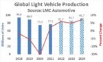
Simultaneous with this slowdown in unit shipments, ASPs fall, hence the plummeting nature of sales value. It’s a deluge, soft landings just don’t happen. This process started in June 2022 and it typically lasts four quarters. Our forecast was based on negative quarter on quarter growth for the second half of 2022 and first half of 2023, with the market bottoming in Q2-2023 and recovering from Q3-2023 onwards. Rolling these quarterly growth numbers forward led to a 22 percent year-on-year decline, 2023 vs. 2022.
Charles: Wow 22 percent decline in 2023. How do we go from here to a 22 percent decline in 2023? Maybe let me ask from a different angle… You said there is no soft landing. Is the path forward more like a V, or a U, or a K?
Malcolm: As mentioned before, the market collapse typically last four quarters and the ensuing recover spans a three to five-year period, so it’s more the shape of a hockey stick on its side. There is nothing to indicate why this current market correction and recovery will be different.
Charles: Based on your current forecast, on a quarterly basis, when will the rate of decline be the greatest? And when will we start to recover?
Malcolm: When I made the forecast back in January 2022, it was based on a Q3-2022 decline of 3.2 percent followed by 10 percent declines in Q4 2022 and Q1-2023, both being, in addition to the correction, seasonally weak quarters, before bottoming out in Q2-2023, with a further 8 percent decline, followed by 2.5 percent growth in Q3 and a 2.5 percent seasonal decline in Q4.
Granted, a 22 percent decline sounds pretty bad but it’s really just a compensation adjustment from 2021’s 26.6 percent growth. Also, when you look historically back at the at the magnitude of previous swings, from the end of the boom to the start of the bust, you see swings ranging from 69 to 21 percentage points, so going from plus 6 or even 10 percent growth in 2022 to minus 22 percent in 2023 is only a swing of 28-32 percentage points, at the historical low end of the range. Corrections, when they do happen are always very steep.
Charles: I believe there are good number of people on the call who want to push back on your very grim view about the road ahead. Let me ask my follow-up questions first. My first follow-up… Many foundries this time have signed LTAs with their customers. Could LTAs smooth the curve a bit there?
Malcolm: Well, that’s certainly the hope, but I think their impact will be disappointing, a negotiating tool at best. They can never compensate for the fact the customers no longer need the product on order so, at best, suppliers may manage to enforce a price penalty and offset the early impact on ASPs but this will only kick the can down the road and drag out the downturn. You cannot force customers to take product they do not need so the impact on unit shipments will be negligible and fab capacity will be underutilized which will trigger an ASP decline.
Firms will also need to think about the long-term marketing impact on their supplier-customer relationship. Forcing their customers too hard now might just result in a lost customer tomorrow.
Charles: My second follow-up… you touched upon this a bit… the equipment demand remains very high and equipment supply is still very tight… we hear lead time for equipment is now 12-18 months. Now we are seeing some cancellation and pushouts from the memory companies, but not so much on the non-memory side. This elevated level of capacity investment… what do you think is going to do to the upcoming downcycle if nobody cancels equipment orders?
Malcolm: No firm ever sees the downturn coming yet, after it happens, it’s always seen has having been inevitable! Push outs and cancellations will eventually follow through, but there’s always a ‘two quarter lag’, up and down. Memory is always the fastest to react, but the other sectors will also soon feel the pain, except at the extreme leading-edge where capacity is always tight.
If firms are part way through a capacity expansion, there is always a point of no return whereby they have no choice but to finish what’s been started, a bit like V1 speed for an aircraft, even though it will exacerbate the excess capacity situation. The spend thus continues after the market has collapsed but eventually capacity expansion plans are adjusted to the new demand reality and which means push outs, cancellations and delays, the bull-whip effect is inevitable.
Charles: My last follow-up… CHIPS Act. The CHIPS Act is now signed into law. What’s your general thought on this government subsidized on-shoring? The funding is going to get allocated and get into capacity investments. What’s your view on that?
Malcolm: This is one area where my European location really comes to the fore and my first piece of advice is to look carefully at the European experience … copy the bits that have worked well and learn from the areas that were less successful.
It’s good that governments around the world have woken up, at least temporarily, to the strategic nature of semiconductors but in general, these initiatives fail to grasp the cause of the problem, namely why did the off-shoring occur in the first place?
What inevitably happens in these situations is the proposed programmes start with where we currently are and focus on essentially ‘band aid’ solutions … patching up the current system, rather than starting the other way around, focusing on what do we want the industry to be like in 20 or so years’ time in the face of all the financial and geo-political issues that need to be addressed.
None of the current industry and political thinking or initiatives even start to address these issues and, whilst government investment in the cash-hungry chip industry is to be welcomed, it will have only limited long-term success unless the reasons chip firms off-shored production in the first place are addressed, especially those once IDM firms who elected to go fabless. A sizable amount of offshored chip production is from firms who have no desire whatsoever to own and operate fabs … anywhere.
In addition, none of these programmes have the support of the end market customer, they are all bottom-up initiatives. From Apple down, there is not a single end-customer championing any on-shoring initiative, nor any customer willing to pay a potential price premium for on-shored product.
Industry needs to collectively address this problem and then tell its respective governments what supportive financial and policy incentives are needed to encourage this top-down demand-driven industry market pull.
For a monthly updates, see Future Horizons’ Semiconductor Monthly Update Report:
https://www.futurehorizons.com/page/137/
For the latest industry outlook, join Future Horizons’ 13 September 2022 Webinar
https://us02web.zoom.us/webinar/register/9216604665338/WN_4vgIAPA9TW6co4Wl-z5zRw
Also read:
EDA Product Mix Changes as Hardware-Assisted Verification Gains Momentum
WEBINAR: A Revolution in Prototyping and Emulation
An EDA AI Master Class by Synopsys CEO Aart de Geus


