Governments worldwide have been paying close attention to alternative energy vehicles recently. Many have launched related electric vehicle subsidy policies, accelerating global sales over recent years.
In 2021 at IAA Mobility in Munich, Germany, many major car manufacturers, including Porsche, showcased their all-electric or related concept cars. In addition to adding more smart driving features, most new vehicles are equipped with extensive digital touch dashboards. The in-vehicle infotainment system, security and anti-hacking technology and the overall efficiency of electric vehicles have also been improved. In the meantime, cloud and edge computing capabilities are tremendously enhanced, epitomized by digital data streaming processing, zonal structure and digitalization level of the device. New energy storage concepts and new-look environmental enhancements, such as material recycling, have also been introduced.
WEBINAR REPLAY: Increasing Security Concerns in IoT Devices
In June 2022, the European Parliament voted to cease the sale of fossil fuel vehicles from 2035. Although this was opposed, it has become common knowledge that electric vehicles will become mainstream in the future. The digital revolution of the automotive industry has also brought an infinite opportunities to memory chip manufacturers. Among the various types of memory chips, the competition for flash memory chips in the automotive market seems to be more intense.
HPC Platform to become the new standard for future cars with Flash memory
The transition from mainstream fossil fuel vehicles to electric vehicles, and now all-electric and driverless vehicles, requires the constant improvement of driver assistance systems (ADAS), which means that automotive chips must continually strive to deliver higher levels of self-driving features and sustainable enhancements of the AI algorithms.
HPC integrates several complex technologies, such as high-performance multi-core chips, in-vehicle operating systems, diversified software systems, high-speed and low-latency communication, functional safety, information security and OTA to satisfy application requirements like high-level autonomous driving and vehicle control. The introduction of HPC represents a fundamental restructuring of the automotive electrical and electronic architecture. Currently, many Tier 1 automotive manufacturers are considering adopting zonal architecture, where the central HPC platform makes the highest-level decision and then transmits data commands and power through domain control units (DCU) scattered in various parts of the vehicle.
Like today’s smartphones, high-end smart cars with enhanced software and hardware are available at higher costs. As a result, customers can enjoy higher-level audio and video facilities and enhanced security. Customers can also purchase an entry-level configured vehicle that meets regulatory requirements at the lowest cost. For car manufacturers, the source of revenue will no longer rely solely on new car sales or repairs and maintenance, but the software and platform customers can freely choose based on tiered pricing. Customers can subscribe to online video streaming on a monthly or annual basis and even purchase related services such as assisted autonomous driving at a one-time makeup price, which will bring additional revenue to car makers.
According to relevant statistics, the automotive HPC market size in 2022 is about $560 million, and it is expected to grow year on year reaching $8.05 billion by 2025. To seize the market, automotive chip developers have launched various new HPC SoCs (system on chip), some of which are even equipped with AI deep learning accelerators, which will collect, analyze and learn automotive-related data, as well as accumulate extensive data databases, to help future algorithms continue to improve. Therefore, memory chips responsible for collecting and storing vast amounts of information have become the cornerstone of the car’s journey to digitization.
Ensuring a Vehicle’s Information Flow Supports the Flash Memory
With the evolution of automobiles to digitalization, the demand for data storage and the transmission of information is getting higher. The flow of information and the reading/processing of data are key elements in the communication between devices. At the same time, OTA acts as a medium for devices to continuously learn and recognize new devices and communication languages. Therefore, the demand for applications such as OTA wireless updates will increase, and OTA-related personal and vehicle information security maintenance and authentication/authorization will become more critical.
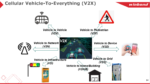
In addition, communicating the flow of information is also required between in-vehicle devices, which created C-V2X (cellular vehicle to everything), a vital role in enhancing road safety, making traffic smoother and saving total energy consumption. As related statistics show, C-V2X is growing at a compound annual growth rate of about 30%. It is estimated that the market will reach $18.8 billion by 2027.
C-V2X is an in-vehicle communication system that includes more specific categories such as V2I (Vehicle-to-Infrastructure), V2N (Vehicle-to-Network), V2V (Vehicle-to-Vehicle), V2P (Vehicle-to-Pedestrian), V2D (Vehicle-to-device) and other information transmission and interpretation between vehicles and different systems or devices. Based on the information flow of these wireless communications, the timely performance and data flow analysis for driving safety is most important.
During this process, all automotive applications require qualified storage products and devices that will endure in embedded environments exposed to extreme temperatures. As a reliable non-volatile memory, NOR flash typically features fast reading speed, high stability, and no data loss when interrupted, which makes it ideal for automotive applications.
WEBINAR REPLAY: Increasing Security Concerns in IoT Devices
However, with the endless increase in the amount of data that devices need to record, such as boot or startup information and user-related information, NAND flash, which has a larger capacity and cost-efficient advantage, gradually revealed its importance.
The Driving Force behind the Automotive Flash Memory Market
After decades of flash memory development, the NOR flash market has already tent to favour niche industries. However, after 2016, the increased demand for consumer electronics and IoT devices with low to medium capacity has led the NOR flash market to pick up and attract new players. The new players have brought NOR Flash into a new era of competition.
From an overall market perspective, benefiting from the rise of emerging application scenarios and the impact of shortages, NOR flash has ushered in a rising cycle. According to an IC Insights report, in the second quarter of 2021, NOR flash only accounted for 4% of the flash memory market. NOR flash products surged by 63% to $2.9 billion last year. NOR flash shipments rose 33 % last year, while average selling prices increased more than 20 %. The NOR flash market is expected to grow another 21% to $3.5 billion in 2022.
However, considering the applications, the current NOR flash is mainly applied in low-capacity applications such as IoT and consumer electronic devices. As competition in this part of the market becomes increasingly fierce, it is easy to fall into a situation where profits diminish. For this reason, major storage manufacturers are trying to break into high-end applications.
The many applications is brought about by the digitalization of automobiles offer opportunities for memory products. According to IC Insights’ statistics on several NOR flash manufacturers’ performance, most NOR flash products’ growth mainly comes from automotive applications. Many manufacturers have seized the automotive market, which has once again activated the vitality of the NOR Flash market.
Winbond is the largest NOR flash supplier, with over $1 billion in sales, accounting for about one-third of the global NOR flash market share. Winbond has been deeply involved in the automotive field for more than ten years as a leading supplier in the NOR flash market. So far, the top ten automobile manufacturers in the world are end customers of Winbond memory products. And their existing niche DRAM, SLC NAND and other product lines have recently expanded their deployment of automotive NOR flash for high-margin product lines.
Winbond Serial NOR Flash has always played a leading role in most automotive applications. However, with the advancement of digitization, the code size that needs to be stored is also increasing. To meet this demand, Winbond launched OctalNAND Flash with 8 I/O ports to fulfil the requirement for instant communication and fast upload and download. Thanks to 8 I/Os, the maximum transmission rate can reach 240MB/s, which can be applied to high-speed and low-latency applications. Octal NOR flash will also join the party shortly.
In addition, Winbond memory products are also suitable for many additional applications, including wireless communication systems, Lidar, tire pressure detectors, in-vehicle wireless charging systems, electric vehicle battery management systems, airbag systems, head-up displays, power management systems and audio systems; as well as the OTA wireless system covering network communication, infotainment and driving recorders. It can support V2X applications, car navigation, digital dashboard, driver monitoring and interactive systems, and it also can be used in gateways, cameras and other in-vehicle fields.
No matter how in-vehicle devices evolve, driving safety will remain a top priority in the automotive industry. Winbond has continuously launched various flash memory products suitable for automotive applications while adhering to the belief of creating high-quality, high-efficiency, low-energy consumption and advanced information security products. Winbond will continue to work closely with automotive manufacturers to fulfil consumers’ wishes.
To learn more, visit Code Storage Flash Memory
Also Read:
The Corellium Experience Moves to EDA
CEVA’s LE Audio/Auracast Solution
VeriSilicon’s AI-ISP Breaks the Limits of Traditional Computer Vision Technologies


