

We looked at another paper on ML-based coverage acceleration back in April 2022. Here is a different angle from IBM. Paul Cunningham (Senior VP/GM, Verification at Cadence), Raúl Camposano (Silicon Catalyst, entrepreneur, former Synopsys CTO and now Silvaco CTO) and I continue our series on research ideas. As always, feedback welcome. And don’t forget to come see us at DVCon, first panel (8am) on March 1st 2023 in San Jose!
The Innovation
This month’s pick is Using DNNs and Smart Sampling for Coverage Closure Acceleration. The authors presented the paper at the 2020 MLCAD Workshop and are from IBM Research in Haifa and the University of BC in Canada.
The authors intent is to improve coverage on events which have been hit only rarely. They demonstrate their method for a CPU design, based on refining instruction set (IS) test templates for an IS simulator. Especially interesting in this paper is how they manage optimization in very noisy low statistics data where conventional gradient-based comparisons are problematic. They suggest several methods to overcome this challenge.
Paul’s view
Here is another paper on using DNNs to improve random instruction generators in CPU verification which, given the rise of Arm-based servers and RISC-V, is becoming an increasingly hot topic in our industry.
The paper begins by documenting a baseline non-DNN method to improve random instruction coverage. This method works by randomly tweaking instruction generator parameters and banking the tweaks if they improve coverage. The tweaking process is based on a gradient-free numerical method called implicit filtering (see here for a good summary), which works kind of like zoom out-then-in search: start with big parameter tweaks and zoom in to smaller parameter tweaks if the big tweaks don’t improve coverage.
The authors then accelerate their baseline method using a DNN to assess if the parameter tweaks will improve coverage before going ahead with costly real simulations to precisely measure the coverage. The DNN is re-trained after each batch of real simulations, so it is continuously improving.
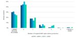
The paper is well written, and the formal justification for their method is clearly explained. Results are presented on two arithmetic pipes of the IBM NorthStar processor (5 instructions and 8 registers). It’s a simple testcase and sims are run for only 100 clock cycles measuring only 185 cover points. Nevertheless, the results do show that the DNN-based method is able to hit all the cover points with half as many sims as the baseline implicit filtering method. Nice result.
Raúl’s view
As Paul says, we are revisiting a topic we have covered before. In April 2022 we reviewed a paper by Google which incorporated a Control-Data-Flow-Graph into a neural network. Back in December 2021we reviewed a paper from U. Gainesville using Concolic (Concrete-Symbolic) testing to cover hard to reach branches. This month’s paper introduces a new algorithm for coverage-directed test generation combining test templates, random sampling, and implicit filtering (IF) with a deep neural network (DNN) model. The idea is as follows:
As is common in coverage directed generation, the approach uses test templates, vectors of weights on a set of test parameters that guide random test generation. Implicit filtering (IF) is an optimization algorithm based on grid search techniques around an initial guess to maximize chances to hit a particular event. To cover multiple events, the IF process is simply repeated for each event, called the parameter-after-parameter approach (PP). To speed up the IF process, the data collected during the IF process is used to train a DNN, which approximates the simulator and is much faster than simulating every test vector.
The effectiveness of the algorithms is evaluated employing an abstract high-level simulator of part of the NorthStar processor. Four algorithms are compared: Random sampling, PP, DNN and combining IF and DNN. The results of three experiments are reported:
- Running the algorithms with a fixed number of test templates, up to 400 runs. Combining IF and DNN is superior, missing only up to 1/3 of the hard to hit events
- Running the algorithms until all hard to hit events are covered. IF and DNN converges with half the number of test templates
- Running the last algorithm (IF and DNN) 5 times. All runs converge with a similar number of test templates, even the worst using ~30% less test templates than other algorithms
This is a well-written paper on a relevant problem in the field. It is (almost) self-contained, it is easy to follow, and the algorithms employed are reproducible. The results show a reduction of “the number of simulations by a factor of 2 or so” over implicit filtering. These results are based on one relatively simple experiment, NorthStar. I would have liked to see additional experimentation and results; some can be found in other publications by the authors.


