
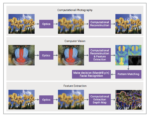
Aberration-free optics are bulky and expensive. Thanks to high-performance AI-enabled processors and GPUs with abundant processing capabilities, image quality nowadays relies more on high computing power tied to miniaturized optics and sensors. Computational imaging is the new trend in imaging and relies on the fusion of computational techniques and traditional imaging to improve image acquisition, processing and visualization. This trend has become increasingly important with the rise of smartphone cameras and involves the use of algorithms, software and hardware components to capture, manipulate and analyze images. It results in improved image quality and enhanced visual information and additionally enables meaningful data extraction which is critical for embedded vision applications.
While there are several advantages from computational imaging, there are many challenges that need to be addressed to enjoy the full potential. The design and simulation tools used by optical designers, electronics engineers, and AI software engineers are often specialized for their respective domains. This creates siloes, hindering collaboration and integration across the entire imaging pipeline and results in suboptimal system performance.
A system-level design and simulation approach that considers the entire imaging system would optimize image quality, system functionality and performance (cost, size, power consumption, latency…). It would require integrating optical design, image sensor and processor design, image processing algorithms and AI models. Synopsys recently published a whitepaper that discusses how the gaps in computational imaging design and simulation pipelines can only be overcome with system-level solutions.
Leveraging AI Algorithms to Improve Computational Imaging Pipeline
Image Signal Processors (ISPs) process raw data from image sensors and perform various tasks to enhance image quality. Traditional ISPs are designed for specific functions and are hardwired for cost efficiency, limiting their flexibility and adaptability to different sensor classes. AI-based image processing utilizing neural networks (NN) shows promise in supplementing or replacing traditional ISPs for improving image quality.
Supplement or Replace Traditional ISPs
For example, a noise filter used in ISPs can enhance image quality but may discard crucial information present in the raw data. By analyzing chromatic aberration effects before digital signal processing (DSP), depth data contained in the raw sensor data can be indirectly extracted. This depth data can then be utilized by AI-based algorithms to reconstruct a 3D representation of a scene from a 2D image, which is not possible with current ISPs. In cases where the primary objective is for computer vision functions to interpret image content using machine learning rather than enhancing perceived quality for human viewing, working with raw data becomes advantageous. Utilizing raw data allows for more accurate object classification, object detection, scene segmentation, and other complex image analyses. In such cases, the presence of an ISP designed for image quality becomes unnecessary.
New Possibilities for Digital Imaging Systems
NNs excel in tasks such as denoising and demosaicing, surpassing the capabilities of traditional ISPs. They can also support more complex features like low-light enhancement, blur reduction, Bokeh blur effect, high dynamic range (HDR), and wide dynamic range. By embedding knowledge of what a good image should look like, NNs can generate higher resolution images. Combining denoising and demosaicing into an integrated process further enhances image quality. Additionally, NN-based demosaicing enables the use of different pixel layouts beyond the conventional Bayer layout, opening up new possibilities for digital imaging systems.
Cheaper Lenses Provide More Accurate Object Detection
NNs can produce better results for certain tasks, such as object detection and depth map estimation, when processing images captured by “imperfect” lenses. As an example, the presence of chromatic aberrations caused by imperfect lenses adds additional information to the image, which can assist the NN in identifying objects and estimating depth.
Co-designing Lens Optics with AI-based Reconstruction Algorithms
While smartphone-based ultra-miniaturized cameras have eclipsed Digital Single Lens Reflex (DSLR) cameras in the market, they face the limits of optics. Researchers at Princeton have explored the use of metalenses, which are thin, flat surfaces that can replace bulky curved lenses in compact imaging applications. They co-designed a metalens with an AI algorithm that corrects aberrations, achieving high-quality imaging with a wide field of view.
The key aspect of this co-design is the combination of a differentiable meta-optical image formation model and a novel deconvolution algorithm leveraging AI. These models are integrated into an end-to-end model, allowing joint optimization across the entire imaging pipeline to improve image quality.
Synopsys Solutions for Designing Imaging Systems
Synopsys offers tools to address the requirements of the entire computational imaging system pipeline. Its optical design and analysis tools include CODE V, LightTools, and RSoft Photonic Device Tools for modeling and optimizing optical systems. The company’s Technology Computer-Aided Design (TCAD) offers a comprehensive suite of products for process and device simulation as well as for managing simulation tasks and results.
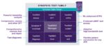
Synopsys also offers a wide range of IP components and development tools to design and evaluate the ISP and computer vision (CV) blocks. These IP components include the MIPI interface, the ARC® VPX family of vector DSPs, and the ARC VPX family of Neural Processing Units (NPUs).
Synopsys ARC MetaWare MX Toolkit provides a common software development tool chain and includes MetaWare Neural Network SDK and MetaWare Virtual Platforms SDK. The Neural Network SDK automatically compiles and optimizes NN models while the Virtual Platforms SDK can be used for virtual prototyping.
Synopsys Platform Architect ™ provides architects and system designers with SystemC™ TLM-based tools and efficient methods for early analysis and optimization of multicore SoC architectures.
Summary
Computational imaging relies more than ever on high computing power tied to miniaturized optics and sensors rather than standalone and bulky but aberration-free optics. Promising system co-design and co-optimization approaches can help unleash the full potential of computational imaging systems by decreasing hardware complexity while keeping computing requirements at a reasonable level.
Synopsys offers design tools for the entire computational imaging pipeline spanning all domains from assisted driving systems in automotive, computer vision-based robots for smart manufacturing or high-quality images for mixed reality.
To access the whitepaper, click here. For more information, contact Synopsys.
Also Read:
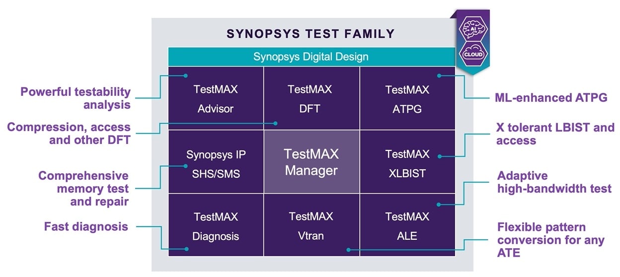
Is Your RTL and Netlist Ready for DFT?
Synopsys Expands Agreement with Samsung Foundry to Increase IP Footprint


