
Modern CPU performance hinges on keeping a processor’s pipeline fed so it executes operations on every tick of the clock, typically using abundant multi-level caching. However, a crop of cache-busting applications is looming, like AI and high-performance computing (HPC) applications running on big data sets. Semidynamics has stepped in with a new highly configurable RISC-V core, Atrevido, including a novel approach to cache misses – the ability to kick off up to 128 independent memory fetches for out-of-order execution.
Experience suggests a different take on moving data
Vector processing has always been a memory-hungry proposition. Various attempts at DMA and gather/scatter controllers had limited success where data could be lined up just right. More often than not, vector execution still ends up being bursty, with a fast vector processor having to pause while its pipeline reloads. Big data applications often introduce a different problem: the data is sparse and can’t be assembled into bigger chunks without expensive moves and lots of waiting. Conventional caching can’t hold all the data being worked on, and what it does hold encounters frequent misses – increasing the wait further.
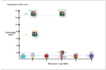
Roger Espasa, CEO and Founder of Semidynamics, has seen the evolution of vector processing firsthand, going back to his days on the DEC Alpha team and followed by a stint at Intel working on what became AVX-512. Their new memory retrieval technology is Gazzillion™, which can dispatch up to 128 simultaneous requests for data anywhere in memory. “It’s tough to glean exactly how many memory accesses some other cores can do from documentation, but we’re sure it’s nowhere near 128,” says Espasa. Despite the difficulty in discovery, his team assembled this look at some competitive cores.
Three important points here. The first is that Gazzillion doesn’t eliminate the latency of any single fetch, but it does hide it when transactions get rolling and subsequent fetches overlap earlier ones in progress. The second is the vector unit in the Atrevido core is an out-of-order unit, which Espasa thinks is a first in the industry. Put those two points together; the result is whichever fetches arrive soonest will be processed next. Finally, the 128 figure is per core. It’s not hard to project this to a sea-of-cores strategy that would provide numbers of execution units with improved fetching needed for machine learning, recommendation systems, or sparse dataset HPC processing.
Way beyond tailorable, fully configurable RISC-V cores match the requirements
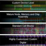
Most RISC-V vendors offer a good list of tailorable features for their cores. Atrevido has been envisioned from the ground up as a fully customizable core where everything is on the table. A customer interview phase determines the application’s needs, and then the core is optimized for power-performance-area (PPA). Don’t need a vector unit? No problem. Change the address space? Sure. Need custom instructions? Straightforward. Coherency, scheduling, or tougher needs? Semidynamics has carved out a unique space apart from the competition, providing customers with better differentiation as they can open up the core for changes – Open Core Surgery, as Espasa enthusiastically terms it. “We can include unique features in a few weeks, and have a customized core validated in a few months,” says Espasa.
An interesting design choice enables more capability. Instead of just an AXI interface, Semidynamics included CHI, allowing Atrevido to plug directly into a coherent network-on-chip (NoC). It’s also process agnostic. Espasa says they have shipped on 22nm and are working on 12nm and 5nm.
Upfront NRE in the interview and optimization phase also has another payoff. Semidynamics can deliver a core for an FPGA bitstream, allowing customers to thoroughly evaluate their customizations before committing a design to a foundry, saving time and reducing risk. Using Semidynamics expertise this way also speeds up exploration without the learning curve of customers having to become RISC-V architectural gurus.
This level of customization means Atrevido fits any RISC-V role, small or large, single or multicore. The transparency of the process helps customers improve their first-pass results and get the most processing in the least area and power. There’s more on the Atrevido announcement, how configurable RISC-V core customization works, and other Semidynamics news at:
https://semidynamics.com/newsroom
Also Read:
Semidynamics: A Single-Software-Stack, Configurable and Customizable RISC-V Solution


