The need for speed is a never-ending story when it comes to data communications. Currently there are a number of trends such as cloud computing, artificial intelligence, Internet of Things (IoT), multimedia applications and consumer expectations driving this demand. All of these trends are accelerating the growth in high-performance-computing (HPC) and the traditional data center server architecture is evolving into a hyper-converged server box architecture. A hyperconverged server box is a type of server infrastructure that combines storage, compute, and networking resources into a single, integrated appliance. It is designed to simplify data center management and reduce infrastructure costs by consolidating multiple functions into a single device. As the industry moves to 224G connectivity rate, there are a number of design considerations and decisions to make to overcome the numerous implementation challenges.
Synopsys’ first demonstration of 224G SerDes was in Basel, Switzerland at the 2022 European Conference on Optical Communication (ECOC). As the first company to demonstrate 224G SerDes, Synopsys has valuable insights to offer. At the recently held IPSoC 2023 conference, Manmeet Walia made a detailed presentation on this subject matter. Manmeet is Director of Product Management at Synopsys for high-speed interface IPs which include PCI-e, Die-to-Die (D2D) and Ethernet.
Why is 224G Ethernet SerDes Needed?
224G Ethernet is needed for a number of reasons. To start with, it is needed for addressing the increasing demand discussed earlier, for higher data rates in modern data centers. The networks within data centers are flattening to reduce latencies, which drives the demand for higher bandwidth connections. Switch SoC die sizes are hitting the maximum reticle size limit, which means the higher connectivity rates are needed to support the higher bandwidth requirement. Server rack unit density, power dissipation and thermal management requirements are also driving the need for 224G connectivity. Additionally, 224G Ethernet helps reduce the number of cables and switches required in high-density data center environments, which can improve network efficiency and reduce costs. In addition, it provides backward compatibility with existing Ethernet standards, allowing for easy integration into existing networks.
Challenges to Delivering 224G
There are several areas of challenges when it comes to implementing and deploying 224G Ethernet. The laws of semiconductor physics are not keeping pace with Serial Link throughout demands. Link loss is going up as package/connector/channel technologies are not keeping pace with the demand. As physical distance on the Front Pluggable Panel has not reduced, reflections get worse. As isolation has not improved, crosstalk gets worse. The overall complexity for implementation increases 5x when increasing speed from 112G to 224G.
Challenges Being Addressed
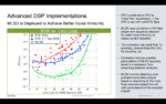
There are a number of aspects to be considered and optimal choices arrived at, starting with the signaling scheme. While the PAM6 scheme delivers less Nyquist loss, PAM4 prevails for most use cases due to better signal-to-noise (SNR) ratio and lower FEC overhead. At the 224G SerDes architecture level, analog circuitry must be minimized for reduced parasitics and high bandwidth front end. And rigorous sensitivity analysis must be performed on individual analog blocks to reduce any impairments. Innovative digital signal processing (DSP) techniques are critical to compensate for the gain errors, skew mismatches and to achieve better noise immunity.
And parallelism should be the theme for high-speed processing efficiency when it comes to the high-level architecture for a 224G SerDes. Optics technology is also moving closer to the host SoC to address power and performance issues as we move to 224G.
Summary
224G Ethernet is fast driving the growth of HPC applications, with the licensing of 224G IP projected to crossover 112G IP by 2025. Early adopter applications include Retimers, Switches, AI Scaling, optical modules, I/O chiplets and FPGAs. Synopsys provides a complete solution with lowest power, area and latency to make it easy for customers to integrate, validate and go to production.
For more details on Synopsys 224G IP, visit here.
To listen to Manmeet’s talk at IPSoC 2023, visit here.
Also Read:
Curvilinear Mask Patterning for Maximizing Lithography Capability
Chiplet Q&A with Henry Sheng of Synopsys
Synopsys Accelerates First-Pass Silicon Success for Banias Labs’ Networking SoC