(First published December 24, 2014)
A list of the best and worst CEOs in 2014 was recently published. The good news is that none of our semiconductor CEOs were on the worst list. The bad news is that none of our semiconductor CEOs were on the best list either. I will be writing about the CEOs that made our industry what it is today starting with the largest and most innovative semiconductor company in the world.
Intel was officially founded in 1968 by Robert Noyce and Gordon Moore (Moore’s Law) with Andy Grove joining as employee number three. These three gentlemen would also be the first three of only eight CEOs over an unprecedented forty six year history. During their thirty year tenure at Intel, Noyce, Moore, and Grove became legends transforming Intel and the entire semiconductor industry into a force of nature that changed the world, absolutely. I would also add Intel CEO number four to that list since Craig Barrett is credited with the now famous Intel “copy exact” manufacturing process that has enabled “Moore’s Law” to continue to this day.
Here are brief bios of the first four Intel CEOs. As you can see there is a common thread amongst their education: PhDs from the top technology academic institutions across the United States.
Robert N. Noyce
Intel CEO, 1968-1975, Co-founder of Fairchild Semiconductor
Education: Ph.D in physics, Massachusetts Institute of Technology
Gordon E. Moore
Intel CEO, 1975-1987, Co-founder of Fairchild Semiconductor
Education: Ph.D in chemistry and physics, California Institute of Technology
Andrew S. Grove
Intel CEO, 1987-1998, previously worked at Fairchild Semiconductor
Education: Ph.D. in chemical engineering, University of California-Berkeley
Craig R. Barrett
Intel CEO, 1998-2005
Joined Intel in 1974, served as chief operating officer from 1993 to 1997, president from 1997 to 1998; chief executive from 1998 through 2005; and chairman from 2005 until 2009.
Education: Ph.D. in materials science, Stanford University
Without Intel where would we be today? We would certainly not have super computing power on our laps nor would we be designing SoCs with FinFETs. As a computer geek since the 1970s and a Silicon Valley based semiconductor professional since the 1980s I have a much better appreciation for Intel than most. I do however fear for their future which is why I am writing this. The problems Intel faces today in my opinion started with an MBA. Who exactly thought that putting a finance guy in charge of the most innovative semiconductor company in the world was a good idea?
Paul S. Otellini
Intel CEO, 2005-2013
Joined the Intel finance department in 1974 . From 1996 to 1998, Otellini served as executive vice president of sales and marketing and from 1994 to 1996 as senior vice president and general manager of sales and marketing.
Education: MBA, University of California-Berkeley, 1974; B.A. in economics, University of San Francisco, 1972
Paul Otellini’s legacy includes two very defining events:
- In 2006 he oversaw the largest round of layoffs in Intel history when 10,500 (10% of the workforce) were laid-off in an effort to save $3 billion per year in costs.
- Also in 2006 he passed on the opportunity to work with Apple on the iPhone.
“We ended up not winning it or passing on it, depending on how you want to view it. And the world would have been a lot different if we’d done it. The thing you have to remember is that this was before the iPhone was introduced and no one knew what the iPhone would do. At the end of the day, there was a chip that they were interested in that they wanted to pay a certain price for and not a nickel more and that price was below our forecasted cost. I couldn’t see it. It wasn’t one of these things you can make up on volume. And in hindsight, the forecasted cost was wrong and the volume was 100x what anyone thought.”
That was the day Intel “missed” mobile. Apple ended up partnering with TSMC which disrupted the foundry business with the half node process development methodology. This new yield learning centric strategy put TSMC solidly in the process technology lead ahead of both semiconductor industry titans Intel and Samsung.
I remember the rumors swirling Silicon Valley after Otellini’s resignation: Would Intel hire an outsider or promote from within? The potential outsider names I heard were very impressive but Intel chose Brian Krazinch, a career Intel employee with zero CEO experience. I was disappointed to say the least.
Brian M. Krzanich
Intel CEO 2013-2018
Began his career at Intel in 1982 in New Mexico as a process engineer and has progressed through a series of technical and leadership roles at Intel, most recently serving as the chief operating officer (COO) since January 2012. Prior to becoming COO, he was responsible for Fab/Sort Manufacturing from 2007-2011 and Assembly and Test from 2003 to 2007. From 2001 to 2003, he was responsible for the implementation of the 0.13-micron logic process technology across Intel’s global factory network. Krzanich also held plant and manufacturing manager roles at multiple Intel factories.
Education: BA in Chemistry from San Jose State University
In 2015-2016 Intel eliminated more than 15,000 jobs companywide which is now the largest downsizing in the company’s history.
“14nm is here, is working, and will be shipping by the end of this year” Brian Kranzich IDF 2013 Keynote. (Intel 14nm officially shipped in 2015).
Intel 14nm was the beginning of the end of Intel’s process technology dominance and at 10nm Intel hit rock bottom. Brian Kranzich was forced out as CEO of Intel for an improper relationship with a co-worker many years prior to becoming CEO. In reality BK was fired for being the worst CEO in the history of Intel, my opinion.
Robert Swan
Intel CEO January 2019-2021
Bob Swan was CEO of Intel Corporation from January 2019 until February 15, 2021. He joined Intel as CFO in October 2016 from General Atlantic, Bob was formerly CFO at eBay, Electronic Data Systems, and TRW. Following the resignation of Brian Krzanich, he was named interim CEO on June 21, 2018, and appointed to full-time CEO on January 31, 2019. Bob was replaced by 30 year Intel employee and former VMware CEO Pat Gelsinger.
Education: Bachelor’s degree in Business Administration from the University of Buffalo, MBA from Binghamton University.
Again, no CEO experience. During Bob’s short reign Intel struck an outsourcing deal with TSMC to support a chiplet strategy which is now in production (Meteor Lake). Intel can use internal fabs or TSMC depending on which is best suited. In my opinion Bob did this as a way to motivate Intel manufacturing as an innovate or die mandate. Some think this is why Bob was fired but, as it turns out, the Intel-TSMC relationship was in fact a pivotal point in the history of Intel.
Pat Gelsinger
Intel CEO 2021-Present
Pat Gelsinger rejoined Intel as CEO on February 15, 2021. He started his career at Intel in 1979, where he spent 30 years in various roles and eventually rose to become the company’s first Chief Technology Officer (CTO). During his tenure at Intel, Gelsinger played a crucial role in the development of several groundbreaking technologies and microprocessors, including the 80486 processor and the original Pentium processor. Before returning to his “dream job” at Intel, Pat was CEO of VMware (2012-2021), a software company specializing in virtualization and cloud computing.
Education: Bachelor’s degree in Electrical Engineering from Santa Clara University, Master’s degree in Electrical Engineering from Stanford University.
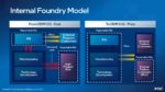
Pat brought Intel back to the forefront of the semiconductor industry with the much heralded Intel IDM (Integrated Device Manufacturing) 2.0 strategy.
Intel IDM 2.0 is a plan introduced by Gelsinger to transform its manufacturing capabilities. It also represents a significant shift in Intel’s approach to manufacturing and involves a combination of strategies aimed at expanding its product portfolio, enhancing competitiveness, and increasing supply chain resilience.
The key elements of Intel IDM 2.0 include:
- Foundry Services: Intel plans to leverage its advanced manufacturing facilities and offer its manufacturing capabilities to external customers through Intel Foundry Services. This initiative aims to become a major player in the foundry business and provide advanced semiconductor manufacturing solutions to a diverse range of industries.
- Internal Product Leadership: Intel continues to prioritize its internal product development and plans to deliver a cadence of leadership products. The focus is on enhancing process technology and driving advancements in chip design to maintain Intel’s position as a leading provider of high-performance and high-efficiency semiconductor solutions.
- Investments in Research and Development: Intel has committed significant investments in research and development to drive innovation and accelerate advancements in semiconductor technologies. This includes investments in next-generation process nodes, packaging technologies, and specialized designs for specific market segments.
- Global Supply Chain Resilience: Intel aims to enhance its supply chain capabilities by diversifying its manufacturing locations and increasing capacity. This strategy is intended to improve responsiveness to market demands, mitigate potential disruptions, and ensure a reliable supply of Intel products.
- Partnerships and Ecosystem Collaboration: Intel recognizes the importance of collaboration and partnerships to drive industry-wide advancements. The company is actively engaging with partners, customers, and governments to foster innovation, develop new technologies, and create a robust ecosystem that supports the growth of the semiconductor industry.
Intel is a changed company with IDM 2.0 which has been covered by SemiWiki in great detail. Pat Gelsinger is a no nonsense – transformative leader with a very large challenge ahead of him. For the sake of Intel and semiconductor manufacturing let’s hope he is successful, absolutely.
Also Read:
VLSI Symposium – Intel PowerVia Technology
IEDM 2022 – Ann Kelleher of Intel – Plenary Talk
Intel Foundry Services Forms Alliance to Enable National Security, Government Applications

