AMD’s Q1-2024 financial results are out, prompting us to delve into the Data Center Processing market. This analysis, usually reserved for us Semiconductor aficionados, has taken on a new dimension. The rise of AI products, now the gold standard for semiconductor companies, has sparked a revolution in the industry, making this analysis relevant to all.
Jenson Huang of Nvidia is called the “Taylor Swift of Semiconductors” and just appeared on CBS 60 Minutes. He found time for this between autographing Nvidia AI Systems and suppliers’ memory products.
Lisa Su of AMD, who has turned the company’s fate, is now one of only 26 self-made female billionaires in the US. Later, she was the CEO of the year in Chief Executive Magazine and has been on the cover of Forbes magazine. Lisa Su still needs to be famous in Formula 1
Hock Tan of Broadcom, desperately trying to avoid critical questions about the change of WMware licensing, would rather discuss the company’s strides in AI accelerator products for the Data Center, which has been significant.
An honorable mention goes to Pat Gelsinger of Intel, the former owner of the Data Center processing market. He has relentlessly been in the media and on stage, explaining the new Intel strategy and his faith in the new course. He has been brutally honest about Intel’s problems and the monumental challenges ahead. We deeply respect this refreshing approach but also deal with the facts. The facts do not look good for Intel.
While the AMD result was challenging from a corporate perspective, the Data Center business, the topic of this article, did better than the other divisions.
The gaming division took a significant decline, leaving the Data Center business as the sole division likely to deliver robust growth in the future. As can be seen, the Data Center business delivered a solid operating profit. Still, it was insufficient to take a larger share of the overall profit in the Data Center Processing market. The 500-pound gorilla in the AI jungle is not challenged yet.
Nvidia’s Q1 numbers have been known for a while (our method is to allocate all of the quarterly revenue in the quarter of the last fiscal month), together with Broadcom’s, the newest entry into the AI processing market. With Intel and AMD’s results, the Q1 overview of the market can be made:
Despite a lower growth rate in Q1-24, Nvidia kept gaining market share, keeping the other players away from the table. Nvidas’ Data Center Processing market share increased from 66.5% to 73.0% of revenue. In comparison, the share of Operating profit declined from 88.4% to 87.8% as Intel managed to get better operating profits from their declining revenue in Q1-24.
Intel has decided to stop hunting low-margin businesses while AMD and Broadcom maintain reasonable margins.
As good consultants, we are never surprised by any development in our area once presented with numbers. That will not stop us from diving deeper into the Data Center Processing supply chain. This is where all energy in the Semiconductor market is concentrated right now.
A CEO I used to work for used to remind me: “When we discuss facts, we are all equal, but when we start talking about opinions, mine is a hell of a lot bigger than yours.”
Our consultancy is built on a foundation of not just knowing what is happening but also being able to demonstrate it. We believe in fostering discussions around facts rather than imposing our views on customers. Once the facts are established, the strategic starting point becomes apparent, leading to more informed decisions.
“There is nothing more deceptive than an obvious fact.” Sherlock Homes
Our preferred tool of analysis is our Semiconductor Market model, seen below:
The model has several different categories that have proven helpful for our analysis and are described in more detail here:
We use a submodel to investigate the Data Center supply chain. This is also an effective way of presenting our data and insights (the “Rainbow” supply and demand indicators) and adding our interpretations as text. Our interpretations can undoubtedly be challenged, but we are okay with that.
Our current findings that the supply chain is struggling to get sufficient CoWoS packaging technology and High Bandwith Memory is not a controversial view and is shared by most that follow the Semiconductor Industry.
This will not stop us from taking a deeper dive to be able to demonstrate what is going on.
The Rainbow bars between the different elements in the supply chain represent the current status.
The interface between Materials & Foundry shows that the supply is high, while the demand from TSMC and other foundries is relatively low.
This supply/demand situation should create a higher inventory position until the two bars align again in a new equilibrium. The materials inventory index does show elevated inventory, and the materials markets are likely some distance away from recovery.
The recent results of the semiconductor tools companies show that revenues are going down, and the appetite of IDMs and foundries indicates that the investment alike is saturated. The combined result can be seen below, along with essential semiconductor events:
The tools market has flatlined since the Chips Act was signed, and there can certainly be a causal effect (something we will investigate in a future post). Even though many new factories are under construction, these activities have not yet affected the tools market.
A similar view of the subcategory of logic tools which TSMC uses shows an even more depressed revenue situation. The tools revenue is back to a level of late 2021, in a time with unprecedented expansion of the semiconductor manufacturing foot print:
This situation is confirmed on the demand side as seen in the TSMC Capital Investments chart below.
Right after the Chips Act was signed, TSMC lowered the capex spend to close to half, making life difficult for the tools manufacturers.
The tools foundry interface has high supply and low demand as could be seen in the supply chain model. The tools vendors are not the limiting factor of GPU AI systems.
To investigate the supply demand situation between TSMC and it’s main customers we choose to select AMD and Nvidia as they have the simplest relationship with TSMC as the bulk of their business is processors made by TSMC.
The inventory situation of the 3 companies can be seen below.
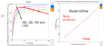
As TSMC’s inventory is building up slightly does not indicate a supply problem however this is TSMC total so their could be other moving parts. The Nvidia peak aligns with the introduction of the H100.
TSMC’s HPC revenue aligns with the Cost of Goods sold of AMD and Nvidia.
As should be expected, these is no surpises in this view. As TSMC’s HPC revenue is growing faster than the COGS of Nvidia and AMD, we can infer that a larger part of revenue is with other customers than Nvidia and AMD. This is a good indication that TSMC is not supply limited from a HPC silicon perspective. Still, the demand is still outstripping supply at the gate of the data centers.
That the skyhigh demand for AI systems is supply is limited, can be seen by the wild operating profit Nvidia is enjoying right no. The supply chain of AI processors looks smooth as we saw before. This is confirmed by the TSMC’s passivity in buying new tools. If there was a production bottle neck, TSMC would have taken action from a tools perspective.
An anlysis of Memory production tools hints at the current supply problem.
The memory companies put the brakes on investments right after the last downcycle began. The last two quarters the demand has increased in anticipation of the High Bandwidth Memory needed for AI.
Hynix in their rececent investor call, confirmed that they had been underinvesting and will have to limit standard DRAM manufacturing in order to supply HBM. This is very visible in our Hynix analysis below.
Apart from the limited supply of HBM, there is also a limitation of advanced packaging capacity for AI systems. As this market is still embryonic and developing, we have not yet developed a good data method to be able to analyze it but are working on it.
While our methods does not prove everything, we can bring a lot of color to your strategy discussions should you decide to engage with our data, insights and models.


