Roger Espasa is the CEO and founder of Semidynamics, an IP supplier of two RISC-V cores, Avispado (in-order) and Atrevido (out-of-order) supporting the RISC-V vector extension and Gazzillion(tm) misses, both targeted at HPC and Artificial Intelligence. Prior to the foundation of the company, Roger was Technical Director/Distinguished Engineer at Broadcom leading a team designing a custom ARMv8/v7 processor on 28nm for the set-top box market. Before its experience at Broadcom, from 2002 to 2014, Roger led various x86 projects at Intel as Principal Engineer: SIMD/vector unit and texture sampler on Knights Ferry (45nm), L2 cache, texture sampler on Knights Corner (22nm), the out-of-order core on Knights Landing (14nm) and the Knights Hill core (10nm). From 1999 to 2001 he worked for the Alpha Microprocessor Group on a vector extension to the Alpha architecture.
Roger got his Phd in Computer Science from Universitat Politècnica de Catalunya in 1997 and has published over 40 peer reviewed papers on Vector Architectures, Graphics/3D Architecture, Binary translation and optimization, Branch Prediction, and Media ISA Extensions. Roger holds 9 patents with 41 international filings.
Tell us about your company?
Processors are my passion. I’ve work on major processor architectures such as Alpha, x86, ARM and now RISC-V. When I became aware of the new RISC-V architecture, I realised that it was going to be the future of processors. Rather than being locked into a choice of either Arm or Intel, companies would have a choice of which IP processor vendor they wanted to use. In addition to vendor-choice, the fact that RISC-V is an open standard means that both customers and vendors can extend the ISA with whatever features they need. This flexibility and this freedom-to-change is something you simply can’t have if you are using Arm or Intel.
So, in 2016, I founded the company and we did a multi-core, RISC-V chip design for Esperanto Technologies. This financed the company as it started up. We had some other design projects that provided the cash flow while we developed our own range of 64-bit RISC-V IP cores such as Atrevido that we announced last year. I am proud to say that we are entirely self-funded through sales and a few European grants which has enabled us to build a dynamic, highly knowledgeable team of over 70 and growing. This means that we are totally in control of our destiny and the pace at which we build the business.
What problems are you solving?
The key problem is that customers have a limited choice when it comes to IP cores, even if you include ARM as a supplier. Furthermore, those IP cores tend to come in a “fixed menu” format, i.e., you can’t add custom features to them. Granted, they all come with some configuration options (cache size, for example), but they can hardly ever be expanded with the customer’s special features needed for their application. We made the decision to accept any change request made by the customer, even if it implied deep “surgery” inside the core. Hence came our motto, “Open Core Surgery”. With us, the customer has total control over the specification, be it new instructions, separate address spaces, new memory accessing capabilities, etc.
This means that Semidynamics can precisely tailor a core to meet each project’s needs so there are no unnecessary overheads or compromises. Even more importantly, Semidynamics can implement a customer’s ‘secret sauce’ instructions and features into the core in a matter of weeks, which is something that no-one else offers.
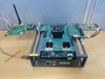
Semidynamics also enables customers to achieve a fast time to market for their customised core as a first drop can be delivered that will run on an FPGA. This enables the customer to check functionality and run software on it while Semidynamics does the core verification. By doing these actions in parallel, the product can be brought to market faster and with reduced risk.
What application areas are your strongest?
We target any application that needs to move massive amounts of data around very fast such as AI and ML. Semidynamics has the fastest cores on the market for moving large amounts of data even when the data does not fit in the cache. Thanks to our “Gazzillion™ technology”, we can sustain a bandwidth of a “cache-line per clock cycle”, i.e., 64 Bytes every clock. And this can be done at frequencies up to 2.4 GHz on the right node. The rest of the market averages about a cache line every many, many cycles; that is nowhere near Semidynamics’ one every cycle. This makes the core perfect for applications that stream a lot of data and/or the application touches very large data that does not fit in cache. This unique capability is thanks to the fact that our cores can support up to 128 simultaneous requests for data and track them back to the correct place in whatever order they are returned. This is nearly 20 times more requests than competitors.
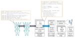
This is ability to move large amounts of data is required by Semidynamics’ Vector Unit that is the largest, fully customisable Vector Unit in the RISC-V market, delivering up to 2048b of computation per cycle for unprecedented data handling. The Vector Unit is composed of several ‘vector cores’, roughly equivalent to a GPU core, that perform multiple calculations in parallel. Each vector core has arithmetic units capable of performing addition, subtraction, fused multiply-add, division, square root, and logic operations. Semidynamics’ vector core can be tailored to support different data types: FP64, FP32, FP16, BF16, INT64, INT32, INT16, INT8, or INT4, depending on the customer’s target application domain. The largest data type size in bits defines the vector core width or ELEN. Customers then select the number of vector cores to be implemented within the Vector Unit, either 4, 8, 16 or 32 cores, catering for a very wide range of power-performance-area trade-off options. Once these choices are made, the total Vector Unit data path width or DLEN is ELEN x number of vector cores. Semidynamics supports DLEN configurations from 128b to 2048b.
Last but not least, our Tensor Unit is built on top of the Semidynamics RVV1.0 Vector Processing Unit and leverages the existing vector registers to store matrices. This enables the Tensor Unit to be used for layers that require matrix multiply capabilities, such as Fully Connected and Convolution, and use the Vector Unit for the activation function layers (ReLU, Sigmoid, Softmax, etc), which is a big improvement over stand-alone NPUs that usually have trouble dealing with activation layers.
The Tensor Unit leverages both the Vector Unit capabilities as well as the Atrevido-423 Gazzillion™ capabilities to fetch the data it needs from memory. Tensor Units consume data at an astounding rate and, without Gazzillion, a normal core would not keep up with the Tensor Unit’s demands. Other solutions rely on difficult-to-program DMAs to solve this problem. Instead, Semidynamics seamlessly integrates the Tensor Unit into its cache-coherent subsystem, opening a new era of programming simplicity for AI software.
Every designer using RISC-V wants to have the perfect set of Power, Performance and Area along with unique differentiating features and now, for the first time, they can have just that. This makes it ideal for the next generation applications of AI, Machine Learning (ML) and High-Performance Computing especially where big data, such as ChatGPT’s 14GB, just won’t fit into L1, L2 or L3 cache.
What keeps your customers up at night?
Finding that their data is too big to be handled with standard core offerings that also struggle to cope with the flow of data. There is a huge demand for AI hardware where this is a major problem. Our solution is the new All-In-One AI IP. This brings together all our innovations to create a unified IP solution that combines RISC-V, Vector, Tensor and Gazzillion technology so that AI chips are now easy to program and scale to whatever processing power is required.
The problem that we address is that the data volume and processing demand of AI is constantly increasing and the current solution is, essentially, to integrate more individual functional blocks. The CPU distributes dedicated partial workloads to gpGPUs (general purpose Graphical Processor Units) and NPUs (Neural Processor Units), and manages the communication between these units. But this has a major issue as moving the data between the blocks creates high latency. The current AI chip configuration is inelegant with typically three different IP vendors and three software tool chains, with poor PPA (Power Performance Area) and is increasingly hard to adapt to new algorithms. For example, they have difficulties handling an AI algorithm called a transformer.
We have created a completely new approach that is easy to program as there is just the RISC-V instruction set and a single software development environment. Integrating the various blocks into one RISC-V AI processing element means that new AI algorithms can easily be deployed without worrying about where to distribute which workload. The data is in the vector registers and can be used by the Vector Unit or the Tensor Unit with each part simply waiting in turn to access the same location as needed. Thus, there is zero communication latency and minimized caches that lead to optimized PPA but, most importantly, it easily scales to meet greater processing and data handling requirements.
In our solution there is just one IP supplier, one RISC-V instruction set and one tool chain making implementation significantly easier and faster with reduced risk. As many of these new processing elements as required to meet the application’s needs can be put together on a single chip to create a next generation, ultra-powerful AI chip.
The RISC-V core inside our All-In-One AI IP provides the ‘intelligence’ to adapt to today’s most complex AI algorithms and even to algorithms that have not been invented yet. The Tensor provides the sheer matrix multiply capability for convolutions, while the Vector Unit, with its fully general programmability, can tackle any of today’s activation layers as well as anything the AI software community can dream of in the future. Having an All-In-One processing element that is simple and yet repeatable solves the scalability problem so our customers can scale from one TOPS to hundreds of TOPS by using as many processing elements as needed on the chip. In addition, our IP remains fully customisable to enable companies to create unique solutions rather than using standard off-the-shelf chips.
What does the competitive landscape look like and how do you differentiate?
There are a lot of competitors and a small handful of big ones but, essentially, they fall in two camps: either they offer a core and, maybe a Vector Unit, or they offer a not-so-flexible NPU. We are unique in providing a fully customisable all-in-one solution comprising a core with our Open Core Surgery, Tensor Unit, Vector Unit and Gazzillion that provide further differentiation to create the high performance, custom core that they need.
What new features/technology are you working on?
One of the many delights of the RISC-V community is that there are always new great ideas being brought into RISC-V. For example, we will be announcing Crypto and Hypervisor in the near future. Plus, of course, a steady stream of new, even more powerful cores.
How do customers normally engage with your company?
For a number of years, it was word of mouth as processor community is relatively small. I have been in it for years so customers sought us out as being RISC-V processor experts that could think outside the box and create exactly the core that they wanted. More recently, we have moved from stealth mode to actively promoting our cores and now we have a growing number of customers from around the world.
Also Read:
Semidynamics Shakes Up Embedded World 2024 with All-In-One AI IP to Power Nextgen AI Chips
RISC-V Summit Buzz – Semidynamics Founder and CEO Roger Espasa Introduces Extreme Customization
Deeper RISC-V pipeline plows through vector-scalar loops