Embargoes and other fun stuff in the Semiconductor Tools Market
While this post dives into the semiconductor tool market’s Q2 data, it is also about the senseless embargo game currently in place. The post illustration shows what my notebooks look like as embargoes enforce what they are supposed to suppress and are replaced by even more restrictive embargoes that… You get the point.
I don’t take sides in the Chip Wars or have an opinion about whether embargoes are needed or justified. I investigate what is going on.
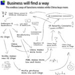
I know that “Business will find a way” (inspired by Michael Crichton’s Jurassic Parc Quote: Life will find a way). The AI part of the embargos has been covered in the post: Pulled out of the black well.
The Semiconductor Tools Market
From a relatively quiet life away from the international spotlight, the Semiconductor Tools companies were propelled onto the geopolitical stage as semiconductors became a matter of national security—first for the US, later for its economic allies, and finally everywhere.
After AI showed its face and made Nvidia a superstar, Non-semiconductor insiders realised that none would be possible without factories in Taiwan and tools from the borderlands of the Nederlands and Belgium.
Despite decades of plentiful investments, the Chinese could not crack the macadamia nut of Semiconductors: Advanced lithography tools.
One company had orchestrated an incredibly advanced R&D effort throughout its supply chain and churned out machines capable of printing the small geometries needed for the most advanced technologies.
The US realised that despite retaining design dominance in Semiconductors, the manufacturing had slipped to Korea and Taiwan and with it, the supply chains.
The Chips Act could stimulate the growth of advanced US manufacturing capacity, but it could do little to remove the reliance on advanced European manufacturing capacity.
Even with the Chips Act, success was not guaranteed as the Chinese had invested in Semiconductor capacity for decades. The US government had to stop the flow of advanced lithography tools to China. Time for embargos.
ASML Embargoes
The US embargoes on AMSL sales to China are delicate as the US has to rely on relationships with the Dutch government. As the ASML sales to China are significant, significant commercial interests are at play.
The embargos started in 2019 with a ban on Extreme UV tools to China capable of better than 7nm processes. These have later been tightened in both 2023 and in the beginning of 2024.
With a mixture of bans and licenses, the embargoes slide from licenses to bans and include more products. As there has been no decline in sales to China, we are likely to see more restrictions over the next period.
The latest development has been debacles between the US and the Nederlands if the embargoes are really driven by national security concerns or more by commercial interest. As a result, the Netherlands have fully aligned to the US restrictions and have taken over the duty of issuing licenses. This is applauded by ASML, which expects a more lenient treatment from the local authorities than the US government.
Before we dive deeper into the outcome of the embargoes, it is worth taking stock of the Semiconductor tools market and its latest results.
The Semiconductor Tools market
Before any chip is made, Semiconductor Tools need to be bought. Throughout the weeks-long journey from blank wafer to finished chip, a multitude of tools is required.
Incredibly simplified, the tools can be categorised as:
- Lithography – the application of the chip design onto the wafer
- Depositions – adding material layers
- Modification – changing material layers
- Removal – removal of material layers
- Other: Metrology, Cleans, Handlers and a multitude of specialised tools.
The tools are placed in the investment zone of our Semiconductor market model and are impacted by the Capital Expenditures of the 3 different categories of Chip manufacturers: IDM’s, Foundries and the FAB/Foundry semiconductor companies.
This is not a business for the faint of heart. A new leading-edge semiconductor fab now costs more than $50B$ to build, and 75% of that cost is tools. The most expensive tools are larger than a double-decker bus and cost more than 350B$
As the geometries become smaller, the chips become cheaper to produce, faster, and consume less power. However, the other side of the coin is that the design costs are skyrocketing, and the tool and factory costs are also increasing.
Comparing the revenue of semiconductor companies with that of tool companies generates the first insights into this development.
The starting point is the bottom of the 2019 semiconductor cycle, and as can be seen, the revenue of the tool companies is outgrowing the semiconductor revenue. The Foundry revenue growth mirrors this. In other words, the collective investment in tools and the manufacturing costs of fabless companies are increasing significantly.
It is not only from a revenue perspective that the tools business is interesting.
From an operating profit perspective, the tools business is more attractive than the foundry and Semiconductor businesses. Notably, most of the semiconductor companies’ Q2-24 profitability stems from Nvidia; without Nvidia, the growth of Semiconductor companies would be a measly 24%.
This is worth noting as an investor as this trend will not change any day soon.
The state of the Semiconductor Tool Companies
The following charts are based on the revenue of semiconductor tool companies, including service and other revenue. The pure tool analysis will follow.
After a growth streak following the latest upcycle, the combined revenue peaks around the introduction of the US Chips Act. This replaces growth with a relatively steady state, with revenues flatlining at around 22B$ and stable Gross and operating profits—nothing to see here.
The declining investments of Semiconductor companies were a direct result of the Chips Act, as projects were redirected to US soil.
This surprised the semiconductor tools companies, or it was too late for them to respond. The result has been an increasing level of inventory that is now double what it was in 2020.
Tool companies used to be concentrated in three countries: the US, Japan, and the Netherlands. At the beginning of the 2020s, only 3% of the revenue was outside these three countries, most of which was in China.
Despite a decade of massive semiconductor investments, these tools proved to be the most difficult to conquer. Success in semiconductor tools requires more than money.
Even after another half-decade, the same countries dominate, although China has worked hard to gain market share. From 3% at the beginning of the decade, China has now managed to get to 8.5% in market share, which is not cause for any celebration in Beijing.
The rapid CAGR growth stopped what was expected during the Chinese New Year of the Dragon but did not bounce back to the levels expected. The inventory position of the Chinese Tools companies indeed suggests that the Chinese tool customers are constipated and not ready to consume at the same levels,
The Chinese tool manufacturers almost exclusively sell to China, but these are not the only tools the Chinese tool customers buy.
The Semiconductor Tool market
After reviewing the Tool companies’ revenue, it is worth investigating the tool revenue of the top companies for more insights. The tool revenue excludes the service and other revenue of Semiconductor tool companies and is perfectly aligned with the CapEx of Semiconductor manufacturing companies.
The dominance of certain countries is due to the domination of a few companies in the Semiconductor tool market.
The top companies account for almost all of the Tool Revenue outside China, and each of the large ones has its own area of specialisation making most of them submarket leaders in subfields, most prominently ASML in lithography and AMAT in materials engineering.
Since introducing the Chips Act and sanctions on AI and advanced lithography tools, sales of Western semiconductor tools to China have exploded.
The revenue of Western tool sold to China grew in Q2 but the Chinese share of revenue declined slightly from 45% in Q1 to 44.4% in Q2. I am sure this is no cause for a victory lap in Washington.
The dominance is even more apparent when compared to revenue from other countries.
The most apparent effect of the Chips act was that TSMC stopped investing in tools as projects were redirected to the US.
Excluding Chinese revenue from the revenue of Western Tool Companies shows the dilemma. China is not only a pain but also a saviour.
This is a crucial problem for the US policy of embargoes. It impacts other countries’ economies, especially when a large company like ASML resides in a small country.
In the last few weeks, there has been a lot of back and forth between Holland and the US government. AMSL has accused the US authorities (in what I cannot believe is not aligned with the Dutch government) of leaning more towards commercial interests than national security interests. At the same time, the Dutch government aligned their restrictions to the US restrictions, so it is now the Dutch authorities that will approve export licenses rather than the US government, something that I am sure ASML is very happy about (I don’t know why…)
China has also threatened Japan with retaliation should the country further sanction tool sales to China.
Conclusion
The US embargoes are focused on preventing the Chinese authorities from accessing leading-edge AI technology. Half of the embargoes are aimed at the GPUs, and the other half are focused on the tools. Memory might be next.
During the last few days, there have been many examples of how easy it is for Chinese companies to buy Nvidia’s H100 or rent it online cheaper than in the West. At the same time, Nvidia’s sales to China are once again increasing despite the embargoes.
The Semiconductor Tools sanctions are in place to prevent the Chinese from gaining access to leading-edge manufacturing technology, which would enable China to make its own GPUs.
The US keeps tightening the sanctions on Semiconductor tools but as with the GPUs, every new sanction seems to enforce what was put in place to inhibit.
I am sure the US authorities are thinking about even more draconian embargos against China, like the Foreign Direct Product Rule that would require the US to dictate all tool sales to China (as they all contain US technology) or try to prevent AMSL and other companies from servicing the existing installed equipment in China.
This would significantly negatively impact ASML and the Dutch economy and would be difficult for the US to get an agreement on.
In this post, I have tried to lay out the result (or lack thereof) of the sanctions in the semiconductor tools market. Tool sales to China remain strong despite increasing embargoes. In my experience, embargoes don’t stop the flow of products; they might change the flow or the cost, but eventually, business will find a way. I accept embargoes might play a political role, but that is not my area of expertise.
I leave you with a chart of Western tool companies’ cumulative sales to China and the US. Since 2019, China has bought nearly $100B worth of Semiconductor tools. More than 2.5 times what the US has bought in the same period. My apologies if that disturbs anybody’s sleep.
KLA Metrology and Inspection
Strong pull from N3 and N2
adv packaging growth from 300m to 500m$ in 2024
Packaging will outgrow WFE
No memory growth yet – will be 2025 and lead by DRAM
KLA share of WFE will grow
DRAM will have higher process control intensity
But it’s not contributing to that they are going to build capacity based on demand. The demand is just going to be based on their market, the overall market, and then they’ll buy equipment accordingly. But we are not counting on our customers to get ChipPAC money to make our plans.
ASML
We also see continued improvement in lithography tool utilization level at both Logic and Memory customers, all in line with the industry’s continued recovery from the downturn.
Lower logic revenue as customers trying to digest last years addition
an increase of EUV use on every node. I think this is a trend that continue at least in the foreseeable future
I think you have seen also in DRAM that this point of time, all customers are using EUV in production
On High NA, we also see opportunity for DRAM at the horizon of ’25, ’26.
LAM
Lam customer investment profile generally unchanged from prior view
+ Slightly stronger domestic China spending
+ Additional demand related to HBM capacity ramp
+ Foundry/logic, DRAM, and NAND investments all expected to be higher on a year-on-year basis
+ Global spending on mature nodes expected to be roughly flat year-on-year
Thanks for reading Semiconductor Business Intelligence! Subscribe for free to receive new posts and support my work.