You are currently viewing SemiWiki as a guest which gives you limited access to the site. To view blog comments and experience other SemiWiki features you must be a registered member. Registration is fast, simple, and absolutely free so please,
join our community today!
In 2012 FinFET is one of the most talked about MOS technologies of the year because traditional planar CMOS has slowed down on scaling below the 28nm node. To learn more about FinFET process modeling I attended a Synopsys webinar where Bari Biswas presented for about 42 minutes include a Q&A portion at the end.
Bari Biswas, Synopsys… Read More
In April I attended and blogged about a webinar on MEMS and IC co-design hosted by two EDA companies: SoftMEMS and Tanner EDA. On October 30th you can attend a full-day event in Israel that is more comprehensive than the webinar that I attended.… Read More
When I think of EDA companies the first geography that comes to mind is Silicon Valley because of the rich history of semiconductor design and fabrication, being close to your customers always makes sense. In the information era it shouldn’t matter so much where you develop EDA tools, so there has been a gradual shift to a wider… Read More
For those of you who didn’t get to DAC you can catch up on low power issues with Apache’s series of low-power webinars taking place late in July. All webinars are at 11am Pacific Time. Full details and registration on the Apache website here.… Read More
I got an email from Mentor Embedded this morning about a webinar on Implementing a GENIVI-compliant System. I have to admit I had no idea what GENIVI is, which surprised me. I spent several years working in the embedded space and so I usually have at least a 50,000 foot view of most things going on there. One reason for my ignorance is … Read More
Collaboration between EDA, Foundry and Design was the key idea today in a webinar hosted by IBM and Cadence about 20nm custom IC design. The three presenters were:
John Stabenow, Cadence
Jeremiah Cessna, Cadence
Keith Barkley, IBM… Read More
While the debate rages on about 28nm yield at foundry juggernaut TSMC, on Monday I attended a webinar on 20nm IC design hosted by TSMC and Synopsys. Double Patterning Technology (DPT) becomes a requirement for several layers of your 20nm IC design which then impact many of your EDA tools and methodology.… Read More
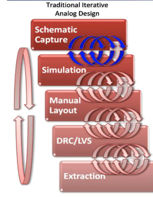
Gim Tan at Magma did a webinar on analog circuit optimization, so I watched it today to see what I could learn about their approach. Gim is a Staff AE, so not much marketing fluff to wade through in this webinar.
The old way of designing custom analog circuits involves many tedious and error prone iterations between front-end (Schematic… Read More
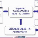
This morning I attended a webinar about MEMS and IC co-design from a company called SoftMEMS along with Tanner EDA. I learned that you can co-design MEMS and IC either in a bottom-up or top-down methodology, and that this particular flow has import/export options to fit in with your mechanical simulation tools (Ansys, Comsol, Open… Read More
I learned about MEMS layout automation at a webinar in December and plan to attend another webinar next week on April 10thwhere two companies have created a MEMS-IC co-design flow, Tanner EDA and SoftMEMS. The big challenge is to ensure that the MEMS and electronic parts of a new design will simulate correctly before committing … Read More


