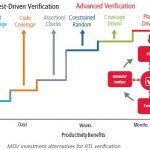
In the current semiconductor design landscape, the design size and complexity of SoCs has grown to large extent with stable tools and technologies that can take care of integrating several IPs together. With that mammoth growth in designs, verification flows are evolving continuously to tackle the verification challenges … Read More
Tag: semiconductor design
Semiconductor Strategy – From Productivity to Profitability
The semiconductor industry seems to be the most challenged in terms of cost of error; a delay of 3 months in product development cycle can reduce revenue by about 27% and that of 6 months can reduce it by almost half; competition is rife, pushing the products to next generation (with more functionality, low power, high performance,… Read More
How to meet 3Ps in 3D-ICs with sub-20nm Dies?
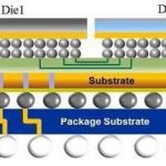
It feels to be at the top of semiconductor technology by having dies with high density of semiconductor design at sub-20nm technology node stacked together into a 3D-IC to form a complete SoC which can accommodate billions of gates. However there are multiple factors to be looked at in order to make that successful amid often conflicting… Read More
Dr. Walden Rhines Vision on Semiconductor & India
Last month India Electronics & Semiconductor Association (IESA) held its Vision Summit at Bangalore in which luminaries from across the semiconductor and electronics industry presented their views about the future of this industry and India’s progress. Dr. Walden C. Rhines, Chairman and CEO of Mentor Graphicspresented… Read More
Mixed-Signal SoC Debugging & IP Integration Made Easy
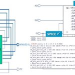
A semiconductor SoC design can have multiple components at different levels of abstractions from different sources and in different languages. While designing an SoC, IPs at different levels have to be integrated without losing the overall design goals. Of course, quality of an IP inside and outside of an SoC must be tested thoroughly.… Read More
A Brief History of Chip Design at Apple Computer
Steve Wozniak in 1976 designed the Apple 1 while working at HP during the daytime, and he used standard parts to keep costs low, like:
- 6502 CPU from MOS Technology
- 8K of DRAM
- TTL logic for driving video and random logic
- PROM to hold the BASIC language and primitive OS
Carbon Design Systems – Secret of Success
Last week, after learning from the press releaseof Carbonabout its rocking sustained growth with record-breaking revenue and a thumping 46% increase in bookings, I was interested to know some more details about what drives Carbon to such an amazing performance in an EDA market that is generally prone to growth of a few percentage… Read More
Smart Strategies for Efficient Testing of 3D-ICs
3D-IC has a stack of dies connected and packaged together, and therefore needs new testing strategies other than testing a single die. It’s given that a single defective die can render the whole of 3D-IC unusable, so each die in the stack must be completely and perfectly tested before its entry into that stack. Looking at it from a … Read More
SoC Verification Closure Pushes New Paradigms
In the current decade of SoCs, semiconductor design size and complexity has grown by unprecedented scale in terms of gate density, number of IPs, memory blocks, analog and digital content and so on; and yet expected to increase further by many folds. Given that level of design, it’s imperative that SoC verification challenge has… Read More
Dual Advantage of Intelligent Power Integrity Analysis
Often it is considered safer to be pessimistic in estimating IR-drop to maintain power integrity of semiconductor designs; however that leads to the use of extra buffering and routing resources which may not be necessary. In modern high speed, high density SoCs having multiple blocks, memories, analog IPs with different functionalities… Read More


