The semiconductor industry seems to be the most challenged in terms of cost of error; a delay of 3 months in product development cycle can reduce revenue by about 27% and that of 6 months can reduce it by almost half; competition is rife, pushing the products to next generation (with more functionality, low power, high performance, more compact, better graphics and much more) in short intervals. This trend has clearly segmented the semiconductor market into design creators (IP vendors focusing on most PPA optimized IPs) and design integrators (SoC vendors focusing on overall quality, cost and time-to-market); fabs with ever shrinking technology node and complexity remaining concentrated among a few with large capital investment capability.
Considering these challenges, the semiconductor companies are focused on improving their processes, developing expertise to handle new complexities, increasing verification coverage to improve quality and so on. While these initiatives definitely improve productivity, today’s business environment needs a greater focus on profitability improvement. Higher cost and reduced profitability has led to mergers of several organizations even though they were productive. It’s no secret, to remain profitable, companies have to be closer to their customers, be collaborative, produce what they require fast and re-use whatever they can, but how?
Last week I was talking to Michael Munsey, Director of Semiconductor Strategy at Dassault Systemes. I was very impressed with the kind of strategy and a broader solution framework they are putting in place to address the issue of productivity and its transformation to profitability in the semiconductor industry. Just to be curious I read into Dassault’s own profitability and that was impressive too; with ~$2.6B revenue and ~31.6% operating margin (Non-IFRS), it’s no wonder Forbes keeps this company in the list of world’s most innovative companies!

So, the idea Dassault has put together seems to be very innovative which relates to the current semiconductor market segmentation and aligns itself with that such that every stakeholder in the design chain (or rather complete product cycle) can gain maximum value out of the product. How’s that possible?
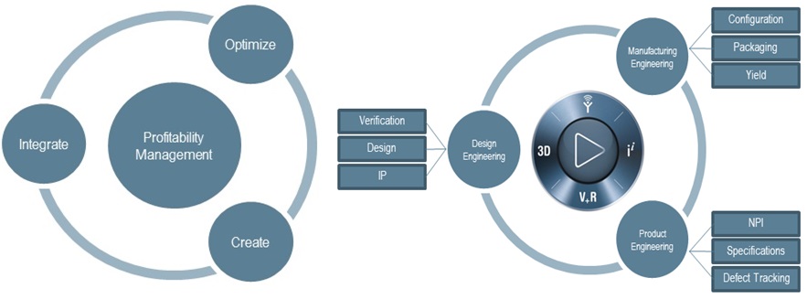
Considering the global business reality the 3DEXPERIENCE platform constituted by Dassault focuses on best design creation, flawless integration and manufacturing optimization that lead to profitability. In order to create best devices, ‘Product Engineering’ framework provides requirement specification management and New Product Introduction (NPI) to develop what customer (or market in broader sense) needs and continuous defect tracking and resolution to remain relevant. ‘Design Engineering’ then manages IPs, their protection, integration of IPs through collaboration between various teams and verification of complete design against the specifications. Finally, ‘Manufacturing Engineering’ works through device configurations, packaging simulations, and analyzing and optimizing yield. The overall platform is geared towards rapid design integration of best devices through highly collaborative environment for analysis, prototyping and optimization, and then cost optimized, risk reduced manufacturing that can generate profit.

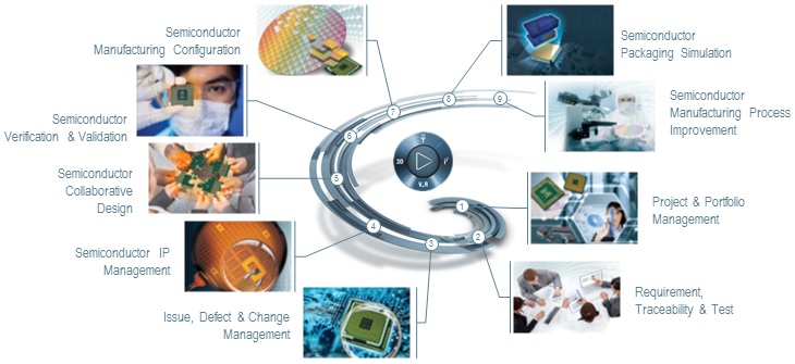
The 3DEXPERIENCEplatform has four major solution spaces. Design Collaboration solution provides ‘Semiconductor Collaborative Design’ that includes issues & defects tracking and change management; requirement, traceability & test; and project & portfolio management. Enterprise IP Management provides ‘Semiconductor IP Management’ that includes issues, defects & change management; requirement, traceability & test; and project & portfolio management. Requirement Driven Verification provides ‘Semiconductor Verification & Validation’ that includes the whole Collaborative Design and IP management pieces along with the common issues, defects & change management; requirement, traceability & test; and project & portfolio management. Then there is Manufacturing Collaboration which provides ‘Semiconductor Manufacturing Configuration’ that includes Semiconductor Packaging Simulation, Semiconductor Manufacturing Process Improvement, project & portfolio management and requirements, traceability & test.
These solution pieces together form a system which checks on wastage of resources and efforts; cost of NPIs, quality processes, misalignments in product and requirements and so on to reduce re-spins, increase re-use and optimize resources thus resulting into profitable business. In future, I will talk more on these individual pieces and exciting stories about how these solutions together address global semiconductor design and manufacturing challenges. Stay tuned!

More Articles by Pawan Fangaria…..
lang: en_US
Share this post via:


Solving the EDA tool fragmentation crisis