


Last week, after learning from the press releaseof Carbonabout its rocking sustained growth with record-breaking revenue and a thumping 46% increase in bookings, I was interested to know some more details about what drives Carbon to such an amazing performance in an EDA market that is generally prone to growth of a few percentage… Read More

Tag: semiconductor design
Smart Strategies for Efficient Testing of 3D-ICs
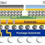
3D-IC has a stack of dies connected and packaged together, and therefore needs new testing strategies other than testing a single die. It’s given that a single defective die can render the whole of 3D-IC unusable, so each die in the stack must be completely and perfectly tested before its entry into that stack. Looking at it from a … Read More
SoC Verification Closure Pushes New Paradigms
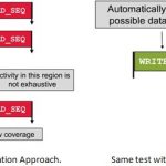
In the current decade of SoCs, semiconductor design size and complexity has grown by unprecedented scale in terms of gate density, number of IPs, memory blocks, analog and digital content and so on; and yet expected to increase further by many folds. Given that level of design, it’s imperative that SoC verification challenge has… Read More
Dual Advantage of Intelligent Power Integrity Analysis
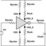
Often it is considered safer to be pessimistic in estimating IR-drop to maintain power integrity of semiconductor designs; however that leads to the use of extra buffering and routing resources which may not be necessary. In modern high speed, high density SoCs having multiple blocks, memories, analog IPs with different functionalities… Read More
RTL Sign-off – At an Edge to become a Standard
Ever since I have seen Atrenta’s SpyGlass platform providing a comprehensive set of tools across the semiconductor design paradigm, I felt the need for a common set of standards to evolve for sign-off at RTL level. Last December, when I read an EE Times articleof Piyush Sancheti, VP, Product Marketing at Atrenta, where he talks … Read More
Parasitic Debugging in Complex Design – How Easy?
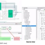
When we talk about parasitic, we talk about post layout design further expanded in terms of electrical components such as resistances and capacitances. In the semiconductor design environment where multiple parts of a design from different sources are assembled together into highly complex, high density SoC, imagine how complex… Read More
Smart Clock Gating for Meaningful Power Saving
Since power has acquired a prime spot in SoCs catering to smart electronics performing multiple jobs at highest speed; the semiconductor design community is hard pressed to find various avenues to reduce power consumption without affecting functionality and performance. And most of the chips are driven by multiple clocks that… Read More
Managing Heat for System Reliability
In most of the electronic equipments, semiconductor chips are a major source of heat generation. And in semiconductor designs several hardware and software techniques are being used to contain power dissipation; a major cause for heat. However due to multiple functionality being squeezed into small form factors, we continue… Read More
How to Develop Accurate Yet High Performance Models
In today’s environment of semiconductor design, SoCs are crammed with various IPs with multiple functionalities and processors integrated together. In such an event it has become necessary to model the system and verify on Virtual Platform before getting into actual design and fabrication. And that requires modelling of each… Read More
Migrating SOCs from 8051 to 32-bits
The 8051 processor has been widely used in many embedded applications over the past 30 years. While the 8051 core is small and simple-to-use, the newest generation of consumer electronics being developed today often require more than the 8051 MCU can reasonably deliver. New SOC applications such as flash drives, power management… Read More