You are currently viewing SemiWiki as a guest which gives you limited access to the site. To view blog comments and experience other SemiWiki features you must be a registered member. Registration is fast, simple, and absolutely free so please,
join our community today!
Gone are the days when analog design had its sweet space on a single chip. However, it’s the main driver in this new electronic world which is geared by Internet-of-Things, wireless, mobile, remote control and so on. How does an electronic device sense a touch by human, motion, temperature, sound etc.? It’s the analog circuitry … Read More
The design and manufacture of MEMS is very different and in many ways more complex process than even the most advanced ICs. MEMS involve multiple degrees of freedom (i.e. the device to exhibit different characteristics under different physical state, motion or mechanics), making fabrication of MEMS extremely complex; and hence… Read More
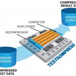
Traditionally ATPG (Automatic Test Pattern Generation) and BIST (Built-In-Self-Test) are the two approaches for testing the whole semiconductor design squeezed on an IC; ATPG requires external test equipment and test vectors to test targeted faults, BIST circuit is implemented on chip along with the functional logic of IC.… Read More
Yes, it is that time of year again, DAC is coming and it is in San Francisco so you can bet we will break attendance records, absolutely. I would like to call on ALL semiconductor IP companies to exhibit this year. IP is the center of the semiconductor design universe, DAC is the premier semiconductor design event, and San Francisco … Read More
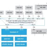
Interconnect plays a significant role in the semiconductor design of a SoC; if not architected and handled well, it can lead to an overdesigned SoC impacting on its power, performance and area. Since a SoC generally contains multiple IPs requiring different data paths to satisfy varying latency and performance cycles, it has … Read More
As power has become one of the most important criteria in semiconductor design today, I was wondering whether there is a standard set for the power verification for an overall chip. We do have formats evolved like CPF and UPF and there are tools available to check power and signal integrity (SI), however I don’t see a standard objective… Read More
In an environment of SoCs with tough targets of multiple functionalities, smallest size, lowest power and fastest performance to achieve within a limited design cycle window in order to meet the rigid time-to-market requirements, any day spent without success becomes very frustrating for a designer. Especially during tape-out… Read More
Now a day, a SoC can be highly complex, having 100s of IPs performing various functionalities along with multi-core CPUs on it. Managing power, performance and area of the overall semiconductor design in the SoC becomes an extremely challenging task. Even if the IPs and various design blocks are highly optimized within themselves,… Read More
As Moore’s law keeps going, semiconductor design density on a chip keeps increasing. The real concern today is that the shrinkage in technology node has rendered the small wire geometry and gate oxide thickness (although fine in all other perspectives) extremely vulnerable to ESD (Electrostatic Discharge) effects. More than… Read More
The growing process integration complexity at each technology node has increased development time and cost, and this trend looks to continue. There is a looming risk of delivering unrepeatable critical unit processes (or process modules) that would require revisiting development and manufacturing requalification or in … Read More