You are currently viewing SemiWiki as a guest which gives you limited access to the site. To view blog comments and experience other SemiWiki features you must be a registered member. Registration is fast, simple, and absolutely free so please,
join our community today!
This week Dr. Eric Esteve, Dr. Bernard Murphy, and I will be blogging live from Arm TechCon. It really looks like it will be a great conference so you should see some interesting blogs in the coming days. One of the topics I am interested in this year is foundation IP and I will tell you why.
During the fabless transformation of the semiconductor… Read More
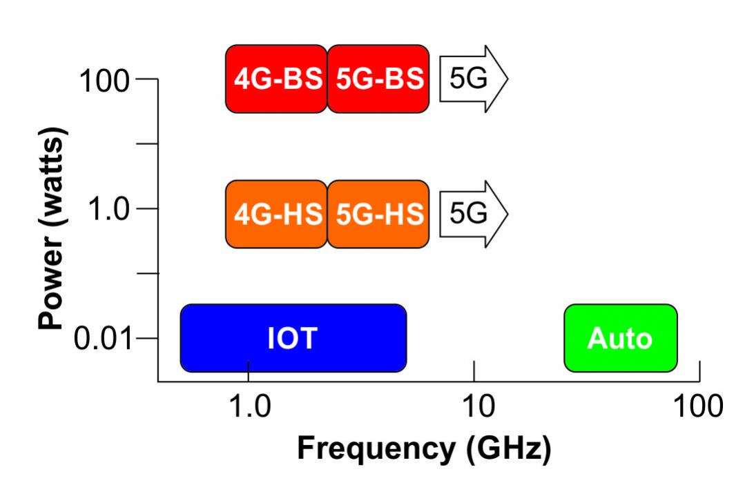
“Mobile is the largest platform ever built by humanity”, Christiano Amon, Executive Vice President, Qualcomm Technologies, Inc. and President, Qualcomm CDMA Technologies speaking at the GLOBALFOUNDRIES Technologies Conference (GTC) 2017.… Read More
The 63rd annual IEDM (International Electron Devices Meeting) will be held December 2nd through 6th in San Francisco. In my opinion IEDM is one of, if not the premier conference on leading edge semiconductor technology. I will be attending the conference again this year and providing coverage for SemiWiki. As a member of the press… Read More
On September 20th GLOBALFOUNDRIES (GF) held their annual technology conference. The conference presented an opportunity to hear the latest on the fascinating journey GF has been on.… Read More
Being the number one EDA and the number one IP company does have its advantages and the resulting foundry relationships are a clear example. One of the DAC traditions that I truly enjoy is the Synopsys foundry breakfasts. Not only does Synopsys welcome scribes, they reserve a table up front for us and Synopsys CEO Aart de Geus has been… Read More
Artificial intelligence, or AI is really heating up these days. The technology has been around for decades, but of late it is becoming quite a focus for applications such as data center analytics, autonomous vehicles and augmented reality. Why the rebirth? The trend appears to be driven by two forces – availability of data to train… Read More
At Semicon West last week I attended presentations by Soitec and CEA Leti, and had breakfast with CEA Leti CEO Marie Semeria, key members of the Fully Depleted Silicon On Insulator (FDSOI) ecosystem. I have also seen some comments in the SemiWiki forum lately that make me believe there is some confusion on the roles of different companies… Read More
I have previously published analysis’ converting leading edge logic processes to “standard nodes” and comparing standard nodes by company and time. Recently updated details on the 7nm process node have become available and in this article, I will revisit the standard node calculations and trends.… Read More
In a SemiWiki EXCLUSIVE – GLOBALFOUNDRIES has now disclosed the key metrics for their 7nm process. As I previously discussed in my 14nm, 16nm, 10nm and 7nm – What we know now blog GLOBALFOUNDRIES licensed their 14nm process from Samsung and decided to skip 10nm because they thought it would be a short-lived node. At … Read More
I have attended last week to the LETI Days in Grenoble, lasting two days to mark the 50[SUP]th[/SUP] anniversary of the CEA subsidiary. Attending to the LETI Days is always a rich experience: LETI is a research center counting about 3000 research engineers, but LETI is also a start-up nursery. The presentations are ranging from … Read More