Having followed GF since its inception, I agree with CTO Gary Patton, what we are seeing today truly is a different GLOBALFOUNDRIES! Our first GF blog was published on 9/13/2009 and we have done a total of 173 GF related blogs that have collected more than 1.5M views thus far. 72 of those blogs were written by me so I have followed this… Read More
Tag: cmos
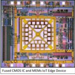
Fusing CMOS IC and MEMS Design for IoT Edge Devices
In my 34 years in IC and EDA, it never ceases to amaze me as to how ingenious designers can be with what is given them. Mentor, a Siemens business, has released a wonderful white paper that is proof of this yet again. The white paper steps through how one of their customers, MEMSIC, used the Tanner tool suite to develop a combination CMOS… Read More
CEO Interview: Jim Gobes of Intrinsix
Experience gives us the ability to make better decisions and in a fast moving industry like semiconductors, experience is critical. As chips get more integrated and complex the number of design decisions that must be made increases at a dramatic rate. Process technologies for example, never in the history of semiconductors have… Read More
Noise, The Need for Speed, and Machine Learning
Technology trends make the concerns with electronic noise a primary constraint that impacts many mainstream products, driving the need for “Design-for-Noise” practices. That is, scaling, and the associated reduction in the device operating voltage and current, in effect magnifies the relative importance of non-scalable… Read More
IoT Devices Making Inroads into Semicon Revenue
Last year IC Insights forecasted IOT semiconductor growth rate to be around 19% CAGR for next five years. And within that space, the O-S-D (Optoelectronics, Sensors, and Discrete) semiconductors were expected to grow at a CAGR of 26%, one among the fastest. In 2015, the O-S-D revenue was at $66.6 billion, i.e. ~19% of total semiconductor… Read More
Coventor prepping MEMS for CMOS integration
About 11 months ago, I wrote a piece titled “Money for data and your MEMS for free.” In that, I took on the thinking that TSMC is just going to ride into town, fab trillions of IoT sensors, and they all will be 2.6 cents ten years from now. Good headline, but the technology and economics are not that simple. This may be the semiconductor … Read More
IEEE S3S Rump Session: “What Does IoT Mean for Si Technology?”
For the second year in the row, Gartner’s Emerging Technologies Hype Cycle puts Internet of Things (IoT) at the Peak of Inflated Expectations. Not only many online forums are inflated with debates on IoT-related topics, but more importantly virtually all semiconductor companies made announcement pertaining their plans to … Read More
Unlock the Key to Ultra-Low Power Design
We have been hearing about low power for a long time. Fortunately, low power chip operation has come about through a large number of innovations. Key among these is clock gating, frequency and voltage scaling, managing leakage with lower threshold voltage, HKMG, and many other techniques. But we are entering the age of ultra low… Read More
Ultra-Low Power Non-Volatile Memory Solutions for the Smart Connected Universe
DAC is a great place to gather information about products and technologies. However it can be difficult to chase down the information you need because you may need to cover a lot of ground to hear or talk to the people with the right knowledge. Fortunately there are a few places you can go to learn about a number of products at one place.… Read More
How Sidense Sees The Smart Connected Universe
Sidenserecently conducted a webinar on what they call the Smart Connected Universe. They consider the Smart Connected Universe as something that includes a collection of market segments that are both smart and connected. This casts a big net, and includes what many are calling IoT, but goes further into medical, automotive and… Read More


