Coventor prepping MEMS for CMOS integration

Coventor prepping MEMS for CMOS integration
by Don Dingee on 10-07-2015 at 12:00 pm

About 11 months ago, I wrote a piece titled “Money for data and your MEMS for free.” In that, I took on the thinking that TSMC is just going to ride into town, fab trillions of IoT sensors, and they all will be 2.6 cents ten years from now. Good headline, but the technology and economics are not that simple. This may be the semiconductor … Read More


IEEE S3S Rump Session: “What Does IoT Mean for Si Technology?”

IEEE S3S Rump Session: “What Does IoT Mean for Si Technology?”
by khaki on 09-20-2015 at 12:00 pm

For the second year in the row, Gartner’s Emerging Technologies Hype Cycle puts Internet of Things (IoT) at the Peak of Inflated Expectations. Not only many online forums are inflated with debates on IoT-related topics, but more importantly virtually all semiconductor companies made announcement pertaining their plans to … Read More


Unlock the Key to Ultra-Low Power Design

Unlock the Key to Ultra-Low Power Design
by Tom Simon on 06-20-2015 at 7:00 am

We have been hearing about low power for a long time. Fortunately, low power chip operation has come about through a large number of innovations. Key among these is clock gating, frequency and voltage scaling, managing leakage with lower threshold voltage, HKMG, and many other techniques. But we are entering the age of ultra low… Read More


Ultra-Low Power Non-Volatile Memory Solutions for the Smart Connected Universe

Ultra-Low Power Non-Volatile Memory Solutions for the Smart Connected Universe
by Tom Simon on 06-01-2015 at 6:00 pm

DAC is a great place to gather information about products and technologies. However it can be difficult to chase down the information you need because you may need to cover a lot of ground to hear or talk to the people with the right knowledge. Fortunately there are a few places you can go to learn about a number of products at one place.… Read More


How Sidense Sees The Smart Connected Universe

How Sidense Sees The Smart Connected Universe
by Tom Simon on 05-17-2015 at 7:00 am

Sidenserecently conducted a webinar on what they call the Smart Connected Universe. They consider the Smart Connected Universe as something that includes a collection of market segments that are both smart and connected. This casts a big net, and includes what many are calling IoT, but goes further into medical, automotive and… Read More


IEDM 2014 Preview

IEDM 2014 Preview
by Scotten Jones on 11-17-2014 at 8:00 pm

The International Electron Devices Meeting (IEDM) is one of the premier conferences for the presentation of the latest semiconductor processes and process technologies. IEDM is held every year in December alternating between San Francisco and Washington DC. This year IEDM will be held at the San Francisco Hilton on December… Read More


TI – The Initial Innovator of Semiconductor ICs

TI – The Initial Innovator of Semiconductor ICs
by Pawan Fangaria on 02-09-2014 at 9:00 am


[TI’s China Foundry acquired from SMIC]

During my engineering graduation, electronic design courses and mini-projects, the ICs I used to come across were SN 7400 series from Texas Instrumentsthat covered a large range of devices from basic gates and flip-flops to counters, registers, memories, ALUs, system controllers, and… Read More


Simulation of Novel TFT Devices

Simulation of Novel TFT Devices
by Paul McLellan on 01-27-2014 at 5:45 pm

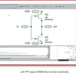
Traditionally logic devices built on top of thin-film-transistors (TFTs) have used one type of device, either an NMOS a-Si: TFT (hydrogenated amorphous silicon) or a PMOS organic device. Recently a-Si:H and pentacene PMOS TFTs have been integrated into complementary logic structures similar to CMOS. This, in turn, creates… Read More


Rapid Yield Optimization at 22nm Through Virtual Fab

Rapid Yield Optimization at 22nm Through Virtual Fab
by Pawan Fangaria on 09-09-2013 at 10:00 am

Remember? During DAC2013 I talked about a new kind of innovation: A Virtual Fabrication Platform, SEMulator3D, developed by COVENTOR. Now, to my pleasant surprise, there is something to report on the proven results from this platform. IBM, in association with COVENTOR, has successfully implemented a 3D Virtual Fabrication… Read More


FinFET Modeling and Extraction at 16-nm

FinFET Modeling and Extraction at 16-nm
by Daniel Payne on 12-18-2012 at 12:05 pm

In 2012 FinFET is one of the most talked about MOS technologies of the year because traditional planar CMOS has slowed down on scaling below the 28nm node. To learn more about FinFET process modeling I attended a Synopsys webinar where Bari Biswas presented for about 42 minutes include a Q&A portion at the end.


Bari Biswas, SynopsysRead More