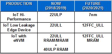
 At TSMC 2018 Silcon Valley Technology Symposium, Dr Kevin Zhang, TSMC VP of Business Development covered technology updates for IoT platform. The three growth drivers in this segment namely TSMC low power, RF enhancement and embedded memory technology (MRAM/RRAM) reinforced both progress and growth in global semiconductor revenue since 1980 –from PC, notebook, mobile phone, smartphone and eventually IoT. For 2017-2022 period, CAGR of 24% and 6.2B units of IoT end devices shipment by 2022 are projected.
RF Technology for IoT Connectivity.
While low power technology unleashes IoT innovation directing shifts from 0.18u eLL/90nm uLP → 55/40 ulP → 22 ULP/ULL → 12 FFC, AI has enabled voice and visual intelligence. Many applications such as voice, AI, audio analysis, surround view sensors and monitoring, etc. require low power technology. Advanced low leakage, embedded SRAM uLL, connectivity plus RF, and advanced eNVM are pillars that further the move to smart society with IoT and AI.
 The current 22ULP/ULL technology offering is based on 28HPC+ manufacturing excellence. TSMC leveraged N28 silicon experience and design ecosystem.
22ULP achieves over 20% power reduction, >10% speed gain and 10% area improvement. It includes uLL device and SRAM with 5% optical shrink and a complete platform. The 22ULL has Triple Gate Oxide (TGO) eHVT, ULL SRAM and eMRAM/RRAM. Good correlation with v0.9 SPICE and PDK specification.
Temperature sensors also introduced to achieve lower Vret and to reduce the retention leakage (1.9pA/cell). Further scaling occured on the nominal voltage to 0.8v and even to 0.6v(!), which is near threshold level requiring the introduction of near Vt sign-off flow and wider range model.
The enablement plan to support 0.6v VDD includes:
– SPICE: extends silicon coverage to sub 0.6v, better analog design for mismatch and 1/f;
– Stdcell: more characterization coverage (sigma adjustment)
– SRAM: compilers to allow dual rails (0.8 for array and 0.6 for peripheral)
– Signoff: advanced signoff methodology (near device Vt)
RF Technology Roadmap
As transceiver operates in less than 6Ghz, the migration will be from 28nm (28LP RF) to either 16nm/12nm FFC-RF for high-end or towards 22ULP-RF for mainstream products. While on the mmWave applications requiring over 24Ghz frequency the shift will be from 28HPC to 22ULP/ULL-RF. The RF front-end is still with 0.13u RF.
22ULP/ULL RF enhancements include increasing unit gain frequency with new RF device, substantially reducing 1/f noise, improving density of passive component (R/C, resistivity improved by a factor of 2x), enhancing analog gain and matching, and rolling-out new 6.5v high voltage device.
Also noted, an excellent fT, mismatch and flicker noise for best IoT connectivity performance. LNA power scaling trend shows around 2X power reduction leveraging transistor performance. mmWave characterization capability expanded from 25 → 50 → 110 Ghz.
MRAM/RRAM are the emerging memories for eNVM. He elaborated on these technologies to contrast them: MRAM utilizes magnetic tunnel junction to move the dipole (spin) whereby changing the resistance and hence, logic value. While RRAM uses conductive filament connected disc to modify the resistance of memory cell. Costwise: eFlash ($$$), MRAM ($$) and RRAM ($). While RRAM is being showcased having the best retention after 1M cycles over 10 years at high temperature.

Additional Details on 16/12FFC_RF
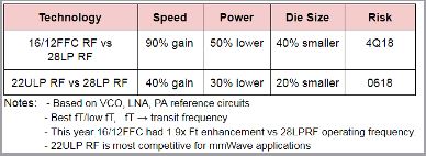
Dr. BJ Woo, TSMC VP of Business Development gave some details for sub 6Ghz applications. TSMC has 16/12FFC-RF and 22ULP RF for 5G mmWave applications which compared to its predecessor 28LP RF showing significant speed-up as captured in the table.

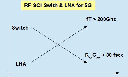
The aggressive trend for Switch and LNA needed for 5G is illustrated in the diagram on left.
Over 100K wafers shipped so far in with these technologies covering >170 tapeouts as they offer best uniformity control and cycle times.
Dr. Cheng-Ming Lin, Director of Business Development of Automotive and MCU reviewed the current state of the automotive market and its mega trends driven by advanced logic technology solutions for ADAS and automotive silicons. He noted a 7.1% CAGR in automotive between 2017-2022, out of which 2.3%is due to vehicle sales (reaching 107M from 96M) and a much higher contribution from its related silicon content of 4.8%.
Breaking down the growth further, he noted the growth number for green applications such as infotainment digital cockpit: 15%, safety related such as environment/vision sensors, airbag: 19% and 9% for smart (AI) context –all of which are required for progressing from the current level 3 status to level 4 (by 2020) and eventually fully autonomous by 2022 (through AI augmentation).
There are three growth drivers in focus: sensors (camera, LIDAR, Radar, ultra sound), advanced technology and actuators (MCUs). Giving more examples, the move from single channel to multichannel communication, mmWave coverage to enable 5G communication and innovation services through connectivity support the migration to a connected world.
Increased demand to meet “green” requirements:
- Shorter charging time: from 0.5 – 8hrs → 0.25hr at 200miles/hr rate
- Less CO2 emission: from 130 → 95 gr/km
- Charging cost: from $250 → $100/kg
On top of these, MCU (eflash) requiring 100Mhz, 100K endurance cycles at 10 years; BCD power of 70-200v with low Rdson and emb.NVM 4Mb; discrete power having shift from IGBT to SiC/GaN with low Rdson, etc.
The technology moves from serving green oriented applications using 28nm (2015) to partial autonomous driving with ADAS & ML using N16 (2017) and eventually highly autonomous with Deep Learning using N7 (2020).
16FFC/N7 Automotive Ecosystem
The robust 16FFC technology has Vcc min down to 0.75v with sufficient margin, experiencing fast DPPM reduction, auto grade-1 qualified on process and foundation IP, 150C SPICE/aging model, IP9000A spec. qualified and ISO26262 certified. N7 PPA, D0 trend and reliability showed 3x density and >65% power improvements, >35% speed gain, Q2-2019 availability and >10 customers engaged with N16/N7.
In the RF technology space, the sub-6Ghz supported by 16FFC while (5G) mmWave is supported by 28HPC+/22ULL. eFlash (MCU) is addressing the green, safety and smart factors with MCU technology migrating from 55nm → 40nm → 28nm. It has >40% CAGR over 5 years and >1M twelve-inch wafers. First 28nm eflash MCU samples to auto industry and target maturityof yield in 1H2019.
Other automotive technology progress
- The adoption of MRAM with excellent data retention and >1M endurance cycles. Currently doing automotive feasibility with more data in 2H2018 and formal report likely next year.
- Automotive CIS application (image/LiDAR, to enable and addressing vision for objects in all driving conditions), High Dynamic Range (HDR), global shutter, NIR (Near Infra Red) sensor with high Quantum Efficiency (QE).
- Automotive BCD and GaN with 0.18 and 0.13u solution for actuator/PMICs; a shift from 0.18BCD SOI → N55 BCD + eflash on SOI with 70-200v features.
Technology Roadmap for Automotive
Design enablement requires process qualification with reliability target zero ppm. In automotive, TDDB (Time Dependent Dielectric Breakdown) is most stringent that TSMC had trouble early on, but managed to overcome N7 TDDB. It met level beyond spec. already (failure rate is <<<0.1%) as captured in TSMC’s ASP (Automotive Service Package), while ASP 2.0 (dubbed "LZ2.0") for early detection and outlier wafer disposition scheduled in 2H18.
16FFC advanced logic – 16nm in mass production with N7 automotive tapeout scheduled Q219. He highlighted TSMC fabs received both IATF-16949 (automotive sector quality management systems) and ISO-14001 (for effective environmental management system) certifications.
As key takeaways, TSMC seems to make great strides in its IoT and Automotive technology offering –to narrow the gap between digital and mixed-signal design in term of density, power and to some extent performance despite all the certification hurdles. Similar to the other segments (HPC, Mobile) it has leveraged lessons learned from its matured process nodes to propel the development progress. Until the next major technology crossroad.


Comments
3 Replies to “TSMC Technologies for IoT and Automotive”
You must register or log in to view/post comments.